Quantcast
Channel: MIT EECS
Viewing all 1281 articles
Browse latest View live

A better device for measuring electromagnetic radiation

$
0
0

Bolometers, devices that monitor electromagnetic radiation through heating of an absorbing material, are used by astronomers and homeowners alike. But most such devices have limited bandwidth and must be operated at ultralow temperatures. Now, researchers say they’ve found a ultrafast yet highly sensitive alternative that can work at room temperature — and may be much less expensive.

The findings, published today in the journal Nature Nanotechnology, could help pave the way toward new kinds of astronomical observatories for long-wavelength emissions, new heat sensors for buildings, and even new kinds of quantum sensing and information processing devices, the multidisciplinary research team says. The group includes EECS Professor and Research Laboratory of Electronics member Dirk Englund, recent MIT postdoc Dmitri Efetov,, Kin Chung Fong of Raytheon BBN Technologies, and colleagues from MIT and Columbia University.

“We believe that our work opens the door to new types of efficient bolometers based on low-dimensional materials,” says Englund, the paper’s senior author. He says the new system, based on the heating of electrons in a small piece of a two-dimensional form of carbon called graphene, for the first time combines both high sensitivity and high bandwidth — orders of magnitude greater than that of conventional bolometers — in a single device.

“The new device is very sensitive, and at the same time ultrafast,” having the potential to take readings in just picoseconds (trillionths of a second), says Efetov, now a professor  at ICFO, the Institute of Photonic Sciences in Barcelona, Spain, who is the paper’s lead author. “This combination of properties is unique,” he says.

The new system also can operate at any temperature, he says, unlike current devices that have to be cooled to extremely low temperatures. Although most actual applications of the device would still be done under these ultracold conditions, for some applications, such as thermal sensors for building efficiency, the ability to operate without specialized cooling systems could be a real plus. “This is the first device of this kind that has no limit on temperature,” Efetov says.

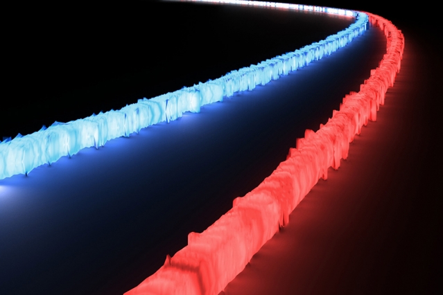
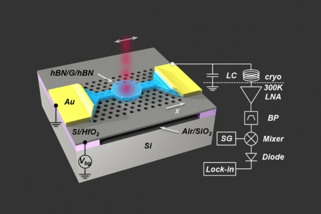
The new bolometer they built, and demonstrated under laboratory conditions, can measure the total energy carried by the photons of incoming electromagnetic radiation, whether that radiation is in the form of visible light, radio waves, microwaves, or other parts of the spectrum. That radiation may be coming from distant galaxies, or from the infrared waves of heat escaping from a poorly insulated house.

The device is entirely different from traditional bolometers, which typically use a metal to absorb the radiation and measure the resulting temperature rise. Instead, this team developed a new type of bolometer that relies on heating electrons moving in a small piece of graphene, rather than heating a solid metal. The graphene is coupled to a device called a photonic nanocavity, which serves to amplify the absorption of the radiation, Englund explains.

“Most bolometers rely on the vibrations of atoms in a piece of material, which tends to make their response slow,” he says. In this case, though, “unlike a traditional bolometer, the heated body here is simply the electron gas, which has a very low heat capacity, meaning that even a small energy input due to absorbed photons causes a large temperature swing,” making it easier to make precise measurements of that energy. Although graphene bolometers had previously been demonstrated, this work solves some of the important outstanding challenges, including efficient absorption into the graphene using a nanocavity, and the impedance-matched temperature readout.

The new technology, Englund says, “opens a new window for bolometers with entirely new functionalities that could radically improve thermal imaging, observational astronomy, quantum information, and quantum sensing, among other applications.”

For astronomical observations, the new system could help by filling in some of the remaining wavelength bands that have not yet had practical detectors to make observations, such as the “terahertz gap” of frequencies that are very difficult to pick up with existing systems. “There, our detector could be a state-of-the-art system” for observing these elusive rays, Efetov says. It could be useful for observing the very long-wavelength cosmic background radiation, he says.

Daniel Prober, a professor of applied physics at Yale University who was not involved in this research, says, “This work is a very good project to utilize the many benefits of the ultrathin metal layer, graphene, while cleverly working around the limitations that would otherwise be imposed by its conducting nature.” He adds, “The resulting detector is extremely sensitive for power detection in a challenging region of the spectrum, and is now ready for some exciting applications.”

And Robert Hadfield, a professor of photonics at the University of Glasgow, who also was not involved in this work, says, “There is  huge demand for new high-sensitivity infrared detection technologies. This work by Efetov and co-workers reporting an innovative graphene bolometer integrated in a photonic crystal cavity to achieve high absorption is timely and exciting.”

For related content about this story, visit the MIT News website.

Date Posted: 

Tuesday, June 12, 2018 - 6:00pm

Labs: 

Card Title Color: 

Black

Card Description: 

The new bolometer is faster, simpler, and covers more wavelengths.

Photo: 

Card Wide Image: 


Novel transmitter protects wireless data from hackers

$
0
0

MIT researchers developed a transmitter that frequency hops data bits ultrafast to prevent signal jamming on wireless devices. Image: Courtesy of the researchers

Rob Matheson | MIT News


Today, more than 8 billion devices are connected around the world, forming an “internet of things” that includes medical devices, wearables, vehicles, and smart household and city technologies. By 2020, experts estimate that number will rise to more than 20 billion devices, all uploading and sharing data online.

But those devices are vulnerable to hacker attacks that locate, intercept, and overwrite the data, jamming signals and generally wreaking havoc. One method to protect the data is called “frequency hopping,” which sends each data packet, containing thousands of individual bits, on a random, unique radio frequency (RF) channel, so hackers can’t pin down any given packet. Hopping large packets, however, is just slow enough that hackers can still pull off an attack.

Now MIT researchers have developed a novel transmitter that frequency hops each individual 1 or 0 bit of a data packet, every microsecond, which is fast enough to thwart even the quickest hackers.

The transmitter leverages frequency-agile devices called bulk acoustic wave (BAW) resonators and rapidly switches between a wide range of RF channels, sending information for a data bit with each hop. In addition, the researchers incorporated a channel generator that, each microsecond, selects the random channel to send each bit. On top of that, the researchers developed a wireless protocol — different from the protocol used today — to support the ultrafast frequency hopping.

“With the current existing [transmitter] architecture, you wouldn’t be able to hop data bits at that speed with low power,” says Rabia Tugce Yazicigil, a postdoc in the Department of Electrical Engineering and Computer Science and first author on a paper describing the transmitter, which is being presented at the IEEE Radio Frequency Integrated Circuits Symposium. “By developing this protocol and radio frequency architecture together, we offer physical-layer security for connectivity of everything.” Initially, this could mean securing smart meters that read home utilities, control heating, or monitor the grid.

“More seriously, perhaps, the transmitter could help secure medical devices, such as insulin pumps and pacemakers, that could be attacked if a hacker wants to harm someone,” Yazicigil says. “When people start corrupting the messages [of these devices] it starts affecting people’s lives.”

Co-authors on the paper are Anantha P. Chandrakasan, dean of MIT’s School of Engineering and the Vannevar Bush Professor of Electrical Engineering and Computer Science (EECS); former MIT postdoc Phillip Nadeau; former MIT undergraduate student Daniel Richman; EECS graduate student Chiraag Juvekar; and visiting research student Kapil Vaidya.

Ultrafast frequency hopping

One particularly sneaky attack on wireless devices is called selective jamming, where a hacker intercepts and corrupts data packets transmitting from a single device but leaves all other nearby devices unscathed. Such targeted attacks are difficult to identify, as they’re often mistaken for poor a wireless link and are difficult to combat with current packet-level frequency-hopping transmitters.

With frequency hopping, a transmitter sends data on various channels, based on a predetermined sequence shared with the receiver. Packet-level frequency hopping sends one data packet at a time, on a single 1-megahertz channel, across a range of 80 channels. A packet takes around 612 microseconds for BLE-type transmitters to send on that channel. But attackers can locate the channel during the first 1 microsecond and then jam the packet.

“Because the packet stays in the channel for long time, and the attacker only needs a microsecond to identify the frequency, the attacker has enough time to overwrite the data in the remainder of packet,” Yazicigil says.

To build their ultrafast frequency-hopping method, the researchers first replaced a crystal oscillator — which vibrates to create an electrical signal — with an oscillator based on a BAW resonator. However, the BAW resonators only cover about 4 to 5 megahertz of frequency channels, falling far short of the 80-megahertz range available in the 2.4-gigahertz band designated for wireless communication. Continuing recent work on BAW resonators — in a 2017 paper co-authored by Chandrakasan, Nadeau, and Yazicigil — the researchers incorporated components that divide an input frequency into multiple frequencies. An additional mixer component combines the divided frequencies with the BAW’s radio frequencies to create a host of new radio frequencies that can span about 80 channels.

Randomizing everything

The next step was randomizing how the data is sent. In traditional modulation schemes, when a transmitter sends data on a channel, that channel will display an offset — a slight deviation in frequency. With BLE modulations, that offset is always a fixed 250 kilohertz for a 1 bit and a fixed -250 kilohertz for a 0 bit. A receiver simply notes the channel’s 250-kilohertz or -250-kilohertz offset as each bit is sent and decodes the corresponding bits.

But that means, if hackers can pinpoint the carrier frequency, they too have access to that information. If hackers can see a 250-kilohertz offset on, say, channel 14, they’ll know that’s an incoming 1 and begin messing with the rest of the data packet.

To combat that, the researchers employed a system that each microsecond generates a pair of separate channels across the 80-channel spectrum. Based on a preshared secret key with the transmitter, the receiver does some calculations to designate one channel to carry a 1 bit and the other to carry a 0 bit. But the channel carrying the desired bit will always display more energy. The receiver then compares the energy in those two channels, notes which one has a higher energy, and decodes for the bit sent on that channel.

For example, by using the preshared key, the receiver will calculate that 1 will be sent on channel 14 and a 0 will be sent on channel 31 for one hop. But the transmitter only wants the receiver to decode a 1. The transmitter will send a 1 on channel 14, and send nothing on channel 31. The receiver sees channel 14 has a higher energy and, knowing that’s a 1-bit channel, decodes a 1. In the next microsecond, the transmitter selects two more random channels for the next bit and repeats the process.

Because the channel selection is quick and random, and there is no fixed frequency offset, a hacker can never tell which bit is going to which channel. “For an attacker, that means they can’t do any better than random guessing, making selective jamming infeasible,” Yazicigil says.

As a final innovation, the researchers integrated two transmitter paths into a time-interleaved architecture. This allows the inactive transmitter to receive the selected next channel, while the active transmitter sends data on the current channel. Then, the workload alternates. Doing so ensures a 1-microsecond frequency-hop rate and, in turn, preserves the 1-megabyte-per-second data rate similar to BLE-type transmitters. 

“Most of the current vulnerability [to signal jamming] stems from the fact that transmitters hop slowly and dwell on a channel for several consecutive bits. Bit-level frequency hopping makes it very hard to detect and selectively jam the wireless link,” says Peter Kinget, a professor of electrical engineering and chair of the department at Columbia University. “This innovation was only possible by working across the various layers in the communication stack requiring new circuits, architectures, and protocols. It has the potential to address key security challenges in IoT devices across industries.”

The work was supported by Hong Kong Innovation and Technology Fund, the National Science Foundation, and Texas Instruments. The chip fabrication was supported by TSMC University Shuttle Program.

.

Date Posted: 

Tuesday, June 12, 2018 - 6:45pm

Labs: 

Card Title Color: 

Black

Card Description: 

The device uses ultrafast “frequency hopping” and data encryption to protect signals from being intercepted and jammed.

Photo: 

Card Wide Image: 

Chip ugrade helps miniature drones navigate

$
0
0

A new computer chip, shown with a quarter for scale, helps miniature drones navigate in flight. Image courtesy of the researchers

Researchers at MIT, who last year designed a tiny computer chip tailored to help honeybee-sized drones navigate, have now shrunk their chip design even further, in both size and power consumption.

The team, co-led by EECS Associate Professor Vivienne Sze and Sertac Karaman, the Class of 1948 Career Development Associate Professor of Aeronautics and Astronautics, built a fully customized chip from the ground up, with a focus on reducing power consumption and size while also increasing processing speed.

The new computer chip, named “Navion,” which they recently presented at the Symposia on VLSI Technology and Circuits, is just 20 square millimeters — about the size of a LEGO minifigure’s footprint — and consumes just 24 milliwatts of power, or about 1 one-thousandth the energy required to power a lightbulb.

Using this tiny amount of power, the chip is able to process in real-time camera images at up to 171 frames per second, as well as inertial measurements, both of which it uses to determine where it is in space. The researchers say the chip can be integrated into “nanodrones” as small as a fingernail, to help the vehicles navigate, particularly in remote or inaccessible places where global positioning satellite data is unavailable.

The chip design can also be run on any small robot or device that needs to navigate over long stretches of time on a limited power supply.

“I can imagine applying this chip to low-energy robotics, like flapping-wing vehicles the size of your fingernail, or lighter-than-air vehicles like weather balloons, that have to go for months on one battery,” says Karaman, who is a member of the Laboratory for Information and Decision Systems and the Institute for Data, Systems, and Society at MIT. “Or imagine medical devices like a little pill you swallow, that can navigate in an intelligent way on very little battery so it doesn’t overheat in your body. The chips we are building can help with all of these.”

Sze and Karaman’s co-authors are EECS graduate student Amr Suleiman, who is the lead author; EECS graduate student Zhengdong Zhang; and Luca Carlone, who was a research scientist during the project and is now an assistant professor in MIT’s Department of Aeronautics and Astronautics.

A flexible chip

In the past few years, multiple research groups have engineered miniature drones small enough to fit in the palm of your hand. Scientists envision that such tiny vehicles can fly around and snap pictures of your surroundings, like mosquito-sized photographers or surveyors, before landing back in your palm, where they can then be easily stored away.

But a palm-sized drone can only carry so much battery power, most of which is used to make its motors fly, leaving very little energy for other essential operations, such as navigation, and, in particular, state estimation, or a robot’s ability to determine where it is in space.  

“In traditional robotics, we take existing off-the-shelf computers and implement [state estimation] algorithms on them, because we don’t usually have to worry about power consumption,” Karaman says. “But in every project that requires us to miniaturize low-power applications, we have to now think about the challenges of programming in a very different way.”

In their previous work, Sze and Karaman began to address such issues by combining algorithms and hardware in a single chip. Their initial design was implemented on a field-programmable gate array, or FPGA, a commercial hardware platform that can be configured to a given application. The chip was able to perform state estimation using 2 watts of power, compared to larger, standard drones that typically require 10 to 30 watts to perform the same tasks. Still, the chip’s power consumption was greater than the total amount of power that miniature drones can typically carry, which researchers estimate to be about 100 milliwatts.

To shrink the chip further, in both size and power consumption, the team decided to build a chip from the ground up rather than reconfigure an existing design. “This gave us a lot more flexibility in the design of the chip,” Sze says.

Running in the world

To reduce the chip’s power consumption, the group came up with a design to minimize the amount of data — in the form of camera images and inertial measurements — that is stored on the chip at any given time. The design also optimizes the way this data flows across the chip.

“Any of the images we would’ve temporarily stored on the chip, we actually compressed so it required less memory,” says Sze, who is a member of the Research Laboratory of Electronics at MIT. The team also cut down on extraneous operations, such as the computation of zeros, which results in a zero. The researchers found a way to skip those computational steps involving any zeros in the data. “This allowed us to avoid having to process and store all those zeros, so we can cut out a lot of unnecessary storage and compute cycles, which reduces the chip size and power, and increases the processing speed of the chip,” Sze says.

Through their design, the team was able to reduce the chip’s memory from its previous 2 megabytes, to about 0.8 megabytes. The team tested the chip on previously collected datasets generated by drones flying through multiple environments, such as office and warehouse-type spaces.

“While we customized the chip for low power and high speed processing, we also made it sufficiently flexible so that it can adapt to these different environments for additional energy savings,” Sze says. “The key is finding the balance between flexibility and efficiency.” The chip can also be reconfigured to support different cameras and inertial measurement unit (IMU) sensors.

From these tests, the researchers found they were able to bring down the chip’s power consumption from 2 watts to 24 milliwatts, and that this was enough to power the chip to process images at 171 frames per second — a rate that was even faster than what the datasets projected.

The team plans to demonstrate its design by implementing its chip on a miniature race car. While a screen displays an onboard camera’s live video, the researchers also hope to show the chip determining where it is in space, in real-time, as well as the amount of power that it uses to perform this task. Eventually, the team plans to test the chip on an actual drone, and ultimately on a miniature drone.

This research was supported, in part, by the Air Force Office of Scientific Research, and by the National Science Foundation.


Date Posted: 

Friday, June 22, 2018 - 12:15pm

Labs: 

Card Title Color: 

Black

Card Description: 

The low-power design will allow devices as small as a honeybee to determine their location while flying.

Photo: 

Card Wide Image: 

CSAIL launches new five-year collaboration with iFlyTek

$
0
0

CSAIL Director Daniela Rus and iFlyTek Chairman/CEO Qingfeng Liu. Photo: CSAIL

The MIT Computer Science and Artificial Intelligence Laboratory (CSAIL) has announced a new five-year collaboration with iFlyTek, a leading Chinese company in the field of artificial intelligence (AI) and natural language processing.

iFlyTek’s speech-recognition technology is often described as “China’s Siri” and is used extensively across multiple industries to translate languages, give directions, and even transcribe court testimony. Alongside Baidu, Alibaba, and Tencent, they are one of four companies designated by the Chinese Ministry of Science and Technology to develop open platforms for AI technologies. Their researchers will collaborate with CSAIL on several projects in fundamental AI and related areas, including computer vision, speech-to-text systems, and human-computer interaction.

“We are very excited to embark on this scientific journey with the innovative minds at iFlyTek,” says CSAIL Director Daniela Rus, the Andrew (1956) and Erna Viterbi Professor of Electrical Engineering and Computer Science at MIT. “Some of the biggest challenges of the 21st century concern developing the science and engineering of intelligence and finding ways to better harness the strengths of both human and artificial intelligence. I am looking forward to the advances that will come from the collaboration between MIT CSAIL and iFlyTek.”

This week CSAIL hosted Qingfeng Liu, chairman and CEO of iFlyTek, as well as Shipeng Li, corporate vice president of iFlyTek and co-president of iFlyTek Research. Representatives from the two organizations talked about the collaboration in more detail and formally signed the research agreement on Thursday.

“We look forward to this exciting collaboration with MIT CSAIL, home of many of the greatest innovations and the world’s brightest talents,” says Liu. “This also shows iFlyTek’s commitment to fundamental research. iFlyTek is applying AI technologies to improve some very important functions of our society, including education, health care, judicature, et cetera. There are no doubt many challenging issues in AI today. We are thrilled to have this opportunity to join hands with MIT CSAIL to push the boundary of AI technology further and to build a better world together.”

Participating researchers from CSAIL include professors Randall Davis, Jim Glass, and Joshua Tenenbaum. Davis will collaborate with iFlyTek on human-computer interaction and creating interfaces to be used in health care applications. Glass’s research will focus on unsupervised speech processing. Tenenbaum’s work will center around trying to build more human-like AI by integrating insights from cognitive development, cognitive neuroscience, and probabilistic programming.


Date Posted: 

Monday, June 18, 2018 - 12:30pm

Labs: 

Card Title Color: 

Black

Card Description: 

The lab will work with the Chinese company on research in artificial intelligence, language processing, and human-computer interaction.

Photo: 

Card Wide Image: 

Phi Beta Kappa Society inducts 28 EECS graduates

$
0
0

The Phi Beta Kappa Society, the nation’s oldest academic honor society, invited 77 graduating seniors from the Class of 2018 into the MIT chapter, Xi of Massachusetts. Twenty-eight EECS-affilated students were among this year's inductees.

Phi Beta Kappa (PBK), founded in 1776 at the College of William and Mary, honors the nation’s most outstanding undergraduate students for excellence in the liberal arts, which include the humanities, the arts, sciences, and social sciences. Only 10 percent of higher education institutions have PBK chapters, and fewer than 10 percent of students at those institutions are selected for membership.

“This year’s inductees have been chosen on the basis of their exceptional academic performance, which has included not just technical subjects but also substantial commitment to the humanities, arts, and social and natural sciences in their purest forms — learning for learning’s sake,” said Arthur Bahr, an associate professor of literature at MIT and the president of Xi of Massachusetts. “Such an education prepares them to thrive not just in particular careers but also in the broader and more important practice of pursuing reflective, meaningful, and well-lived lives."

At the induction ceremony, which took place on June 7, Allan Adams, principal investigator of the Future Oceans Lab at MIT, presented an address entitled, “On the Value of Invisible Things.” Allen discussed his professional transition from a theoretical string physicist to a passionate oceanographic researcher intent on exploring and conserving the world’s oceans. In describing what he’s learned from “lifting the veil” and discovering the vast invisible life hidden within ocean depths, he advised the new inductees to “keep an eye out for invisible things to guide you and drive you.” As Allen observed, “Exploring involves risk — whether in space, your career, or your heart.”

Bahr, who specializes in medieval literature, provided the inductees and their families with a lively overview of the “ancient … well, relatively ancient" PBK society. With assistance from chapter historian Anne McCants, professor of history, and chapter guardian Elizabeth Vogel Taylor of the Concourse Program and the Department of Chemistry, Bahr introduced the 2018 inductees to the rights and responsibilities of PBK members. The inductees were then recognized individually, shown the society’s secret handshake, and signed the register of the Xi of Massachusetts chapter.

Congratulations to:

  • Akkas Abdurrahaman, EECS, Konya, Turkey
  • Lotta-Gili Blumberg, EECS and Physics, Springfield, New Jersey
  • Kelsey Chan, EECS, Palo Alto, California
  • Siqi Chen, EECS, Nanjing, Jiangsu, China
  • Hannah Diehl, EECS, Beverly Hills, Michigan
  • Arezu Esmaili, EECS, Stony Brook, New York
  • Michael Feffer, EECS, Boalsburg, Pennsylvania
  • Arkadiy Frasinich, EECS, Oak Park, Michigan
  • Julian Fuchs, EECS, Davis, California
  • Courtney Guo, EECS, Cambridge, Massachusetts
  • Joseph Lin, EECS, State College, Pennsylvania
  • Carolyn Lu, EECS, Carlisle, Massachusetts
  • Tarek Mansour, EECS and Mathematics, Jounieh, Lebanon
  • Edgar Minasyan, EECS, Yerevan, Armenia
  • Weerachai Neeranartvong, EECS and Mathematics, Washington, D.C.
  • Edward Park, EECS and Mathematics, Suwanee, Georgia
  • Rajeev Parvathala, EECS and Mathematics, Phoenix, Arizona
  • Nipun Pitimanaaree, EECS and Mathematics, Washington, D.C.
  • Oliver Ren, EECS and Mathematics, San Diego, California
  • Sophia Russo, EECS, Santa Barbara, California
  • Claire Simpson, EECS, St. Louis Park, Minnesota
  • Nat Sothanaphan, EECS and Mathematics, Washington, D.C.
  • Fransisca Susan, EECS and Mathematics, Jakarta, Indonesia
  • Kyle Swanson, EECS and Mathematics, Bronxville, New York
  • Rachel Thornton, EECS, Medfield, Massachusetts
  • Henry Wu, EECS and Mathematics, Toronto, Ontario, Canada
  • Rachel Yang, EECS and Music and Theater Arts, Moraga, California
  • Liang Zhou, EECS and Brain and Cognitive Sciences, Carlsbad, California


Date Posted: 

Wednesday, June 27, 2018 - 2:30pm

Card Title Color: 

Black

Card Description: 

In all, 77 members of MIT's Class of 2018 were invited to join the prestigious honor society.

Photo: 

Constantinos Daskalakis wins prestigious Nevanlinna Prize

$
0
0

Professor Costis Daskalakis.                                                                                Photo: Courtesy of Professor Daskalakis

Adam Conner-Simon | CSAIL


EECS Professor Constantinos (“Costis”) Daskalakis has won the 2018 Rolf Nevanlinna Prize, one of the most prestigious international awards in mathematics.

Announced at the International Conference of Mathematicians in Brazil, the prize is awarded every four years (alongside the Fields Medal) to a scientist under 40 who has made major contributions to the mathematical aspects of computer science.

Daskalakis, also a principal investigator the Computer Science and Artificial Intelligence Laboratory (CSAIL), was honored by the International Mathematical Union (IMU) for “transforming our understanding of the computational complexity of fundamental problems in markets, auctions, equilibria, and other economic structures," according to the citation. The award comes with a monetary prize of 10,000 euros.

"Costis combines amazing technical virtuosity with the rare gift of choosing to work on problems that are both fundamental and complex,” says CSAIL Director Daniela Rus. “We are all so happy to hear about this well-deserved recognition for our colleague.”

A native of Greece, Daskalakis received his undergraduate degree from the National Technical University of Athens and his PhD in electrical engineering and computer sciences from the University of California at Berkeley. He has previously received such honors as the 2008 ACM Doctoral Dissertation Award, the 2010 Sloan Fellowship in Computer Science, the Simons Investigator Award from the Simons Foundation, and the Kalai Game Theory and Computer Science Prize from the Game Theory Society.

Created in 1981 by the Executive Committee of the IMU, the prize is named after the Finnish mathematician Rolf Nevanlinna. The prize is awarded for outstanding contributions on the mathematical aspects of informational sciences. Recipients are invited to participate in the Heidelberg Laureate Forum, an annual networking event that also includes recipients of the ACM A.M. Turing Award, the Abel Prize, and the Fields Medal.


Date Posted: 

Wednesday, August 1, 2018 - 5:45pm

Card Title Color: 

Black

Card Description: 

The EECS professor is honored for his contributions to theoretical computer science.

Photo: 

Card Wide Image: 

Research Area: 

MITx introductory Python course hits 1.2 enrollments

$
0
0

Since it was conceived as an online offering in 2012, the MITx massive open online course (MOOC), Introduction to Computer Science using Python, has become the most popular MOOC in MIT history with 1.2 million enrollments to date.

The course is derived from a campus-based and Open CourseWare subject at MIT developed and originally taught at MIT by John Guttag, the Dugald C. Jackson Professor of Computer Science and Electrical Engineering. “Although on the surface it’s a computer programming course with Python, it’s really not about Python or even programming,” explains Guttag. “It’s about teaching students to use computation, in this case described by Python, to build models and explore broader questions of what can be done with computation to understand the world.”

The first MITx version of this course, launched in 2012, was co-developed by Guttag and Eric Grimson, the Bernard M. Gordon Professor of Medical Engineering and professor of computer science. It was one of the very first MOOCs offered by MIT on the edX platform.

“This course is designed to help students begin to think like a computer scientist,” says Grimson. “By the end of it, the student should feel very confident that given a problem, whether it’s something from work or their personal life, they could use computation to solve that problem.”

The course was initially developed as a 13-week course, but in 2014 it was separated into two courses, 6.00.1x and 6.00.2x. “We achieved 1.4 million enrollments at the beginning of the summer with both courses combined,” says Ana Bell, lecturer in electrical engineering and computer science, who keeps the MOOC current by adding new problem sets, adding exercises, and coordinating staff volunteer teaching assistants (TAs). “At its core, the 6.00 series teaches computational thinking,” adds Bell. “It does this using the Python programming language, but the course also teaches programming concepts that can be applied in any other programming language.” 

Enrollment is already high for the next 6.001x course, which starts today. Guttag, Grimson, and Bell suggest several reasons for the course’s popularity. For example, many learners are older or are switching careers and either have not been exposed to computer science much or are looking for new skills. “Many learners take it because they see computer science as a path forward and something they need to know,” says Grimson. 

Providing new lives for refugees

Such is the case of Muhammad Enjari, a 39-year-old petroleum engineer from Homs, Syria. He fled Homs with his wife and 3 children at the beginning of the Syrian revolution and settled in Jordan soon after. “I have a degree in petroleum engineering but in Jordan I could not find a job,” he says.

In his journey to jumpstart a new career, Enjari enrolled in 6.00.1x as part of the MIT Refugee Action Hub, or ReACT, a yearlong Computer and Data Science Program (CDSP) curriculum. He received a 100 percent on the final exam and a 100 percent final grade. “Because of this course and others, I will be starting a new job in two weeks as a paid intern in computer engineering with Edraak, a MOOC platform similar to edX for Arabic-speaking students,” he adds.

Similarly, when 23-year-old Manda Awad, another ReACT CDSP student, enrolled in the 6.00.1x course as a refugee from Palestine living in Jordan, she learned that some of the material/topics covered in the course series was not included in her computer science curriculum at the University of Jordan. This, coupled with a lack of support for women in tech, inspired Awad to write a proposal that would update the engineering department’s computer science curricula by integrating the 6.00 series coursework, and expand access to the material across the student body. “I want to take what I have learned and teach other students, particularly women,” she says. Awad is currently setting up a programming club with a weekly instructional segment. She has a goal of introducing a “Women who Code” group to the Zaatari refugee camp in Jordan, which she plans to launch in the next year.

Expanding career options

Grain farmer Matt Reimer of Manitoba, Canada, enrolled in the course to develop a computer program to improve his farm’s efficiency, productivity, and profitability. He gained the skills needed to use remote-control technology to accelerate harvest production using his farm’s auto-steering tractor integrated with his grain combine harvester. The result: The driverless tractor unloaded grain from the combine over 500 times, saving the farm an estimated $5,000 or more.

When Ruchi Garg decided to re-enter the workplace after being the primary caretaker for her two young children, she enrolled in the course to get her former technology career moving again. She was worried that her skillset had grown stale in the wake of rapidly advancing technologies and evolving computer engineering practices. After completing 6.00.1x, Garg has gone on to become a data analyst at The Weather Company, an IBM subsidiary.

Aditi, a blind data security professional based in India, enrolled in 6.00.1x to help create the next generation of security tools. The MIT course was the first completely accessible course she had ever taken online. After finishing the 6.00 series, Aditi will be attending Georgia Tech in the fall for her master’s degree.

And in 2017, MITx partnered with Silicon Valley-based San Jose City College to offer the course as part of a program for students in the area who traditionally have not had access to computer science curriculum. When students complete the course, they are matched with prospective employers for internships and possible employment in the area’s technology industry.

Past students stay involved

Because of her own enthusiasm with the course, Estefania Cassingena Navone became a Community TA for MITx from Venezuela. She has written several supporting documents with visualizations to demystify some of the more complex ideas in the course. “This course gave me the hope I needed,” she says. “Hope that living in a developing country would not be a barrier to achieve what I truly want to achieve in life, it gave me the opportunity to be part of an online community where hard work and dedication really helps you thrive.” 

After taking the course, MITx TA Thomas Ballatore felt empowered to learn more about using computers for his own teaching. Although he has already earned a PhD, he has entered a master’s program majoring in digital media design learning how to produce his own online courses. “I became a TA because of my love of teaching and knew that the best way to truly learn material is to explain it to others.” Now on his fourth cycle of assisting, he has created several tutorial videos, motivated by helping others get their ‘ah-hah’ moments as well.

“This course essentially embodies the MIT spirit of drinking from the firehose,” says Ana Bell. “It's a tough course and fast-paced. If you get through it, you are rewarded with an immense feeling of accomplishment.” And perhaps, also, a new life-changing opportunity.

For more on this story, including a video from MIT Open Learning, visit the MIT News website.

Date Posted: 

Friday, August 31, 2018 - 3:30pm

Card Title Color: 

Black

Card Description: 

Since its 2012 launch, the course has become the most popular MOOC in MIT history, enrolling students from all over the world.

Photo: 

Card Wide Image: 

A 'GPS for inside your body'

$
0
0

Professor Dina Katabi is leading the team developing ReMix. Photo: Simon Simard

Investigating inside the human body often requires cutting open a patient or swallowing long tubes with built-in cameras. But what if physicians could get a better glimpse in a less expensive, invasive, and time-consuming manner?

A team from MIT’s Computer Science and Artificial Intelligence Laboratory (CSAIL) led by Dina Katabi, Andrew & Erna Viterbi Professor of EECS, is working on doing exactly that with an “in-body GPS" system dubbed ReMix. The new method can pinpoint the location of ingestible implants inside the body using low-power wireless signals. These implants could be used as tiny tracking devices on shifting tumors to help monitor their slight movements.

In animal tests, the team demonstrated that they can track the implants with centimeter-level accuracy. The team says that, one day, similar implants could be used to deliver drugs to specific regions in the body.

ReMix was developed in collaboration with researchers from Massachusetts General Hospital (MGH). The team describes the system in a paper that's being presented at this week's Association for Computing Machinery's Special Interest Group on Data Communications (SIGCOMM) conference in Budapest, Hungary.

Tracking inside the body

To test ReMix, Katabi’s group first implanted a small marker in animal tissues. To track its movement, the researchers used a wireless device that reflects radio signals off the patient. This was based on a wireless technology that the researchers previously demonstrated to detect heart rate, breathing, and movement. A special algorithm then uses that signal to pinpoint the exact location of the marker.

Interestingly, the marker inside the body does not need to transmit any wireless signal. It simply reflects the signal transmitted by the wireless device outside the body. Therefore, it doesn't need a battery or any other external source of energy.

A key challenge in using wireless signals in this way is the many competing reflections that bounce off a person's body. In fact, the signals that reflect off a person’s skin are actually 100 million times more powerful than the signals of the metal marker itself.

To overcome this, the team designed an approach that essentially separates the interfering skin signals from the ones they're trying to measure. They did this using a small semiconductor device, called a “diode,” that mixes signals together so the team can then filter out the skin-related signals. For example, if the skin reflects at frequencies of F1 and F2, the diode creates new combinations of those frequencies, such as F1-F2 and F1+F2. When all of the signals reflect back to the system, the system only picks up the combined frequencies, filtering out the original frequencies that came from the patient’s skin.

One potential application for ReMix is in proton therapy, a type of cancer treatment that involves bombarding tumors with beams of magnet-controlled protons. The approach allows doctors to prescribe higher doses of radiation, but requires a very high degree of precision, which means that it’s usually limited to only certain cancers.

Its success hinges on something that's actually quite unreliable: a tumor staying exactly where it is during the radiation process. If a tumor moves, then healthy areas could be exposed to the radiation. But with a small marker like ReMix’s, doctors could better determine the location of a tumor in real-time and either pause the treatment or steer the beam into the right position. (To be clear, ReMix is not yet accurate enough to be used in clinical settings. Katabi says a margin of error closer to a couple of millimeters would be necessary for actual implementation.)

"The ability to continuously sense inside the human body has largely been a distant dream," says Romit Roy Choudhury, a professor of electrical engineering and computer science at the University of Illinois, who was not involved in the research. "One of the roadblocks has been wireless communication to a device and its continuous localization. ReMix makes a leap in this direction by showing that the wireless component of implantable devices may no longer be the bottleneck."

Looking ahead

There are still many ongoing challenges for improving ReMix. The team next hopes to combine the wireless data with medical data, such as that from magnetic resonance imaging (MRI) scans, to further improve the system’s accuracy. In addition, the team will continue to reassess the algorithm and the various tradeoffs needed to account for the complexity of different bodies.

"We want a model that's technically feasible, while still complex enough to accurately represent the human body," says MIT PhD student Deepak Vasisht, lead author on the new paper. "If we want to use this technology on actual cancer patients one day, it will have to come from better modeling a person's physical structure."

The researchers say that such systems could help enable more widespread adoption of proton therapy centers. Today, there are only about 100 centers globally.

"One reason that [proton therapy] is so expensive is because of the cost of installing the hardware," Vasisht says. "If these systems can encourage more applications of the technology, there will be more demand, which will mean more therapy centers, and lower prices for patients."

Katabi and Vasisht co-wrote the paper with MIT PhD student Guo Zhang, University of Waterloo professor Omid Abari, MGH physicist Hsaio-Ming Lu, and MGH technical director Jacob Flanz

For more on this story, including a CSAIL video, visit the MIT News website.

Date Posted: 

Tuesday, August 21, 2018 - 1:45pm

Card Title Color: 

Black

Card Description: 

A CSAIL team led by EECS faculty member Dina Katabi envisions a future where doctors could implant sensors to track tumors or even dispense drugs.

Photo: 

Card Wide Image: 


Muriel Medard discusses the world-altering growth of 5G

$
0
0

Muriel Médard, Cecil H. Green Professor in EECS. Photo: Lillie Paquette, School of Engineering


Editor's Note: The rise of 5G, or fifth-generation, mobile technologies, is reshaping the wireless communications and networking industry. The School of Engineering recently asked Muriel Médard, the Cecil H. Green Professor in the EECS Department, to explain what that means and why it matters.

Médard, the co-founder of three companies to commercialize network coding — CodeOn, Steinwurf, and Chocolate Cloud — is considered a global technology leader. Her work in network coding, hardware implementation, and her original algorithms have received widespread recognition and awards. At MIT, Médard leads the Network Coding and Reliable Communications Group at the Research Laboratory for Electronics.

Q. People are hearing that 5G will transform industries across the world and bring advances in smart transportation, health care, wearables, augmented reality, and the internet of things. The media report that strategic players in the U.S. and internationally are developing these technologies for market by 2020 or earlier. What sets this generation apart from its predecessors?

A. The reason 5G is so different is that what exactly it will look like is still up in the air. Everyone agrees the phrase is a bit of a catch-all. I’ll give you some big brush strokes on 5G and what people are looking at actively in the area.

In second, third, and fourth generations, people got a phone service that by 4G really became a system of phone plus data. It was all fairly traditional. For instance, people are used to switching manually from their cellular provider to available Wi-Fi at their local coffee shop or wherever.

One of the main ideas behind 5G is that you’ll have a single network that allows a blended offering. People are looking at using a multi-path approach, which means drawing on Wi-Fi and non-Wi-Fi 5G (or sometimes 4G) seamlessly. This poses some difficult coordination problems. It requires network coding, by using algebraic combinations, across different paths to create a single, smooth experience.

Another important part of 5G is that people are looking at using millimeter waves, which occupy frequencies that are high enough to avoid interference among multiple senders that are transmitting simultaneously in fairly close proximity relative to what is possible now. These high frequencies, with wide open spectrum regions, may be well-suited for very large amounts of data that need to be transmitted over fairly short distances.

There is also what people call “the fog,” which is something more than just how people feel in the morning before coffee. Fog computing, in effect, involves extending cloud capabilities, such as compute, storage and networking services, through various nodes and IoT gateways. It involves being able to draw on the presence of different users nearby in order to establish small, lightweight, rapidly set-up, rapidly torn-down, peer-to-peer type networks. Again, the right coding is extremely important so that we don't have difficult problems of coordination. You must be able to code across the different users and the different portions of the network.

Q. You’ve described 5G as actively looking at incorporating services and modes of communications that have not been part of traditional offerings. What else sets it apart?

A. Let’s talk about global reach. With 5G, people are looking at incorporating features, such as satellite service, that are seamlessly integrated with terrestrial service. For this, we also really need reliance on coding. You can imagine how there is no way you can rely on traditional coordination and scheduling across satellites and nodes on the ground on large scale.

Another thing that makes 5G so different from other evolutions is the sheer volume of players. If you were talking about 3G or 4G, it was pretty straightforward. Your key players were doing equipment provisioning to service providers.

Now it’s a very busy and more varied set of players. The different aspects that I’ve talked about are often not all considered by the same player. Some people are looking at worldwide coverage via satellite networking. Other people are looking at blending new channels, such as the millimeter wave ones I referred to earlier, with Wi-Fi, which basically requires marrying existing infrastructure with new ones.

I think finding a coherent and central source of information is a big challenge. You have the organization that governs cellular standards, 3GPP, but the whole industry is transforming as we watch in the area of 5G. It’s not clear whether it’s going to be 3GPP still calling the shots. You have so many new entrants that are not necessarily part of the old guard.

Q. What do you believe people will notice on a daily level with the rise of 5G?

A. I’ll give you my vision for the future of 5G, with the caveat that we’re now moving into an area that is more a matter of opinion. I see heterogeneity as part of the design. You're going to have a network that is talking to a large and disparate set of nodes with very different purposes for very different applications. You’re going to see a view that emphasizes integration of existing and new resources over just the deployment of new resources.

And I think the people who are going to win in 5G may not be the same players as before. It will be the company that figures out how to provide people with a seamless experience using the different substrates in a way that is highly opportunistic. It has to be a system that integrates everything naturally because you cannot preplan the satellite beam you're going to be in, the fog network you're going to be in, and the IoT devices that are going to be around you. There is no way even to maintain or manage so much information. Everything is becoming too complex and, in effect, organic. And my view on how to do that? Network coding. That’s an opinion but it’s a strongly held one.

For related content, visit the MIT News website.


Date Posted: 

Monday, August 13, 2018 - 7:00am

Research Theme: 

Labs: 

Card Title Color: 

Black

Card Description: 

The EECS faculty member describes how fifth-generation mobile technologies are revolutionizing the wireless communications and networking industry.

Photo: 

Card Wide Image: 

EECS researchers develop molecular clock that could greatly improve smartphone navigation

$
0
0

Image courtesy of the researchers


MIT researchers have developed the first molecular clock on a chip, which uses the constant, measurable rotation of molecules — when exposed to a certain frequency of electromagnetic radiation — to keep time. The chip could one day significantly improve the accuracy and performance of navigation on smartphones and other consumer devices.

Today’s most accurate time-keepers are atomic clocks. These clocks rely on the steady resonance of atoms, when exposed to a specific frequency, to measure exactly one second. Several such clocks are installed in all GPS satellites. By “trilaterating” time signals broadcast from these satellites — a technique like triangulation, that uses 3-D dimensional data for positioning — your smartphone and other ground receivers can pinpoint their own location.

But atomic clocks are large and expensive. Your smartphone, therefore, has a much less accurate internal clock that relies on three satellite signals to navigate and can still calculate wrong locations. Errors can be reduced with corrections from additional satellite signals, if available, but this degrades the performance and speed of your navigation. When signals drop or weaken — such as in areas surrounded by signal-reflecting buildings or in tunnels — your phone primarily relies on its clock and an accelerometer to estimate your location and where you’re going.

Researchers from EECS and Terahertz Integrated Electronics Group have now built an on-chip clock that exposes specific molecules — not atoms — to an exact, ultrahigh frequency that causes them to spin. When the molecular rotations cause maximum energy absorption, a periodic output is clocked — in this case, a second. As with the resonance of atoms, this spin is reliably constant enough that it can serve as a precise timing reference.  

In experiments, the molecular clock averaged an error under 1 microsecond per hour, comparable to miniature atomic clocks and 10,000 times more stable than the crystal-oscillator clocks in smartphones. Because the clock is fully electronic and doesn’t require bulky, power-hungry components used to insulate and excite the atoms, it is manufactured with the low-cost, complementary metal-oxide-semiconductor (CMOS) integrated circuit technology used to make all smartphone chips.

“Our vision is, in the future, you don’t need to spend a big chunk of money getting atomic clocks in most equipment. Rather, you just have a little gas cell that you attached to the corner of a chip in a smartphone, and then the whole thing is running at atomic clock-grade accuracy,” says Ruonan Han, an associate professor in EECS and co-author of a paper describing the clock, published today in Nature Electronics.

The chip-scale molecular clock can also be used for more efficient time-keeping in operations that require location precision but involve little to no GPS signal, such as underwater sensing or battlefield applications.

Joining Han on the paper are: Cheng Wang, a PhD student and first author; Xiang Yi, a postdoc; and graduate students James Mawdsley, Mina Kim, and Zihan Wang, all from EECS.

In the 1960s, scientists officially defined one second as 9,192,631,770 oscillations of radiation, which is the exact frequency it takes for cesium-133 atoms to change from a low state to high state of excitability. Because that change is constant, that exact frequency can be used as a reliable time reference of one second. Essentially, every time 9,192,631,770 oscillations occur, one second has passed.

Atomic clocks are systems that use that concept. They sweep a narrow band of microwave frequencies across cesium-133 atoms until a maximum number of the atoms transition to their high states — meaning the frequency is then at exactly 9,192,631,770 oscillations. When that happens, the system clocks a second. It continuously tests that a maximum number of those atoms are in high-energy states and, if not, adjusts the frequency to keep on track. The best atomic clocks come within one second of error every 1.4 million years.

In recent years, the U.S. Defense Advanced Research Projects Agency has introduced chip-scale atomic clocks. But these run about $1,000 each — too pricey for consumer devices. To shrink the scale, “we searched for different physics all together,” Han says. “We don’t probe the behavior of atoms; rather, we probe the behavior of molecules.”

The researchers’ chip functions similarly to an atomic clock but relies on measuring the rotation of the molecule carbonyl sulfide (OCS), when exposed to certain frequencies. Attached to the chip is a gas cell filled with OCS. A circuit continuously sweeps frequencies of electromagnetic waves along the cell, causing the molecules to start rotating. A receiver measures the energy of these rotations and adjusts the clock output frequency accordingly. At a frequency very close to 231.060983 gigahertz, the molecules reach peak rotation and form a sharp signal response. The researchers divided down that frequency to exactly one second, matching it with the official time from atomic clocks.

“The output of the system is linked to that known number — about 231 gigahertz,” Han says. “You want to correlate a quantity that is useful to you with a quantity that is physical constant, that doesn’t change. Then your quantity becomes very stable.”

A key challenge was designing a chip that can shoot out a 200-gigahertz signal to make a molecule rotate. Consumer device components can generally only produce a few gigahertz of signal strength. The researchers developed custom metal structures and other components that increase the efficacy of transistors, in order to shape a low-frequency input signal into a higher-frequency electromagnetic wave, while using as little power as possible. The chip consumes only 66 milliwatts of power. For comparison, common smartphone features — such as GPS, Wi-Fi, and LED lighting —can consume hundreds of milliwatts during use.

The chips could be used for underwater sensing, where GPS signals aren’t available, Han says. In those applications, sonic waves are shot into the ocean floor and return to a grid of underwater sensors. Inside each sensor, an attached atomic clock measures the signal delay to pinpoint the location of, say, oil under the ocean floor. The researchers’ chip could be a low-power and low-cost alternative to the atomic clocks.

The chip could also be used on the battlefield, Han says. Bombs are often remotely triggered on battlefields, so soldiers use equipment that suppresses all signals in the area so the bombs won’t go off. “Soldiers themselves then don’t have GPS signals anymore,” Han says. “Those are places when an accurate internal clock for local navigation becomes quite essential.”

Currently, the prototype needs some fine-tuning before it’s ready to reach consumer devices. The researchers currently have plans to shrink the clock even more and reduce the average power consumption to a few milliwatts, while cutting its error rate by another one or two orders of magnitude.

This work was supported by a National Science Foundation CAREER award, MIT Lincoln Laboratory, MIT Center of Integrated Circuits and Systems, and a Texas Instruments Fellowship.

For related content, please visit the MIT News website.

Date Posted: 

Wednesday, July 25, 2018 - 1:30pm

Card Title Color: 

Black

Card Description: 

The novel chip keeps time using the constant, measurable rotation of molecules as a timing reference.

Photo: 

On-chip optical filter processes wide range of light wavelengths

$
0
0


MIT researchers have designed an optical filter on a chip that can process optical signals from across an extremely wide spectrum of light at once, something never before available to integrated optics systems that process data using light. The technology may offer greater precision and flexibility for designing optical communication and sensor systems, studying photons and other particles through ultrafast techniques, and in other applications.

Optical filters are used to separate one light source into two separate outputs: one reflects unwanted wavelengths — or colors — and the other transmits desired wavelengths. Instruments that require infrared radiation, for instance, will use optical filters to remove any visible light and get cleaner infrared signals.

Existing optical filters, however, have tradeoffs and disadvantages. Discrete (off-chip) “broadband” filters, called dichroic filters, process wide portions of the light spectrum but are large, can be expensive, and require many layers of optical coatings that reflect certain wavelengths. Integrated filters can be produced in large quantities inexpensively, but they typically cover a very narrow band of the spectrum, so many must be combined to efficiently and selectively filter larger portions of the spectrum.

Researchers from MIT’s Research Laboratory of Electronics have designed the first on-chip filter that, essentially, matches the broadband coverage and precision performance of the bulky filters but can be manufactured using traditional silicon-chip fabrication methods.

“This new filter takes an extremely broad range of wavelengths within its bandwidth as input and efficiently separates it into two output signals, regardless of exactly how wide or at what wavelength the input is. That capability didn’t exist before in integrated optics,” says Emir Salih Magden, a former PhD student in MIT’s Department of Electrical Engineering and Computer Science (EECS) and first author on a paper describing the filters published today in Nature Communications.

Paper co-authors along with Magden, who is now an assistant professor of electrical engineering at Koç University in Turkey, are: Nanxi Li, a Harvard University graduate student; and, from MIT, graduate student Manan Raval; former graduate student Christopher V. Poulton; former postdoc Alfonso Ruocco; postdoc associate Neetesh Singh; former research scientist Diedrik Vermeulen; Erich Ippen, the Elihu Thomson Professor in EECS and the Department of Physics; Leslie Kolodziejski, a professor in EECS; and Michael Watts, an associate professor in EECS.

Dictating the flow of light

The MIT researchers designed a novel chip architecture that mimics dichroic filters in many ways. They created two sections of precisely sized and aligned (down to the nanometer) silicon waveguides that coax different wavelengths into different outputs.

Waveguides have rectangular cross-sections typically made of a “core” of high-index material — meaning light travels slowly through it — surrounded by a lower-index material. When light encounters the higher- and lower-index materials, it tends to bounce toward the higher-index material. Thus, in the waveguide light becomes trapped in, and travels along, the core.

The MIT researchers use waveguides to precisely guide the light input to the corresponding signal outputs. One section of the researchers’ filter contains an array of three waveguides, while the other section contains one waveguide that’s slightly wider than any of the three individual ones.

In a device using the same material for all waveguides, light tends to travel along the widest waveguide. By tweaking the widths in the array of three waveguides and gaps between them, the researchers make them appear as a single wider waveguide, but only to light with longer wavelengths. Wavelengths are measured in nanometers, and adjusting these waveguide metrics creates a “cutoff,” meaning the precise nanometer of wavelength above which light will “see” the array of three waveguides as a single one.

In the paper, for instance, the researchers created a single waveguide measuring 318 nanometers, and three separate waveguides measuring 250 nanometers each with gaps of 100 nanometers in between. This corresponded to a cutoff of around 1,540 nanometers, which is in the infrared region. When a light beam entered the filter, wavelengths measuring less than 1,540 nanometers could detect one wide waveguide on one side and three narrower waveguides on the other. Those wavelengths move along the wider waveguide. Wavelengths longer than 1,540 nanometers, however, can’t detect spaces between three separate waveguides. Instead, they detect a massive waveguide wider than the single waveguide, so move toward the three waveguides.

“That these long wavelengths are unable to distinguish these gaps, and see them as a single waveguide, is half of the puzzle. The other half is designing efficient transitions for routing light through these waveguides toward the outputs,” Magden says.

The design also allows for a very sharp roll-off, measured by how precisely a filter splits an input near the cutoff. If the roll-off is gradual, some desired transmission signal goes into the undesired output. Sharper roll-off produces a cleaner signal filtered with minimal loss. In measurements, the researchers found their filters offer about 10 to 70 times sharper roll-offs than other broadband filters.

As a final component, the researchers provided guidelines for exact widths and gaps of the waveguides needed to achieve different cutoffs for different wavelengths. In that way, the filters are highly customizable to work at any wavelength range. “Once you choose what materials to use, you can determine the necessary waveguide dimensions and design a similar filter for your own platform,” Magden says.

Sharper tools

Many of these broadband filters can be implemented within one system to flexibly process signals from across the entire optical spectrum, including splitting and combing signals from multiple inputs into multiple outputs.

This could pave the way for sharper “optical combs,” a relatively new invention consisting of uniformly spaced femtosecond (one quadrillionth of a second) pulses of light from across the visible light spectrum — with some spanning ultraviolet and infrared zones — resulting in thousands of individual lines of radio-frequency signals that resemble “teeth” of a comb. Broadband optical filters are critical in combining different parts of the comb, which reduces unwanted signal noise and produces very fine comb teeth at exact wavelengths.

Because the speed of light is known and constant, the teeth of the comb can be used like a ruler to measure light emitted or reflected by objects for various purposes. A promising new application for the combs is powering “optical clocks” for GPS satellites that could potentially pinpoint a cellphone user’s location down to the centimeter or even help better detect gravitational waves. GPS works by tracking the time it takes a signal to travel from a satellite to the user’s phone. Other applications include high-precision spectroscopy, enabled by stable optical combs combining different portions of the optical spectrum into one beam, to study the optical signatures of atoms, ions, and other particles.

In these applications and others, it’s helpful to have filters that cover broad, and vastly different, portions of the optical spectrum on one device.

“Once we have really precise clocks with sharp optical and radio-frequency signals, you can get more accurate positioning and navigation, better receptor quality, and, with spectroscopy, get access to phenomena you couldn’t measure before,” Magden says.

The new device could be useful, for instance, for sharper signals in fiber-to-the-home installations, which connect optical fiber from a central point directly to homes and buildings, says Wim Bogaerts, a professor of silicon photonics at Ghent University. “I like the concept, because it should be very flexible in terms of design,” he says. “It looks like an interesting combination of ‘dispersion engineering’ [a technique for controlling light based on wavelength] and an adiabatic coupler [a tool that splits light between waveguides] to make separation filter for high and low wavelengths.”


Date Posted: 

Tuesday, August 7, 2018 - 1:45pm

Labs: 

Card Title Color: 

Black

Card Description: 

The silicon-based system offers a smaller, cheaper alternative to other “broadband” filters and could improve a variety of photonic devices.

Photo: 

Card Wide Image: 

More efficient security for cloud-based machine learning

$
0
0

Image: Chelsea Turner


A novel encryption method devised by MIT researchers secures data used in online neural networks, without dramatically slowing their runtimes. This approach holds promise for using cloud-based neural networks for medical-image analysis and other applications that use sensitive data.

Outsourcing machine learning is a rising trend in industry. Major tech firms have launched cloud platforms that conduct computation-heavy tasks, such as, say, running data through a convolutional neural network (CNN) for image classification. Resource-strapped small businesses and other users can upload data to those services for a fee and get back results in several hours.

But what if there are leaks of private data? In recent years, researchers have explored various secure-computation techniques to protect such sensitive data. But those methods have performance drawbacks that make neural network evaluation (testing and validating) sluggish — sometimes as much as million times slower — limiting their wider adoption.

In a paper presented at this week’s USENIX Security Conference, MIT researchers describe a system that blends two conventional techniques — homomorphic encryption and garbled circuits — in a way that helps the networks run orders of magnitude faster than they do with conventional approaches.

The researchers tested the system, called GAZELLE, on two-party image-classification tasks. A user sends encrypted image data to an online server evaluating a CNN running on GAZELLE. After this, both parties share encrypted information back and forth in order to classify the user’s image. Throughout the process, the system ensures that the server never learns any uploaded data, while the user never learns anything about the network parameters. Compared to traditional systems, however, GAZELLE ran 20 to 30 times faster than state-of-the-art models, while reducing the required network bandwidth by an order of magnitude.

One promising application for the system is training CNNs to diagnose diseases. Hospitals could, for instance, train a CNN to learn characteristics of certain medical conditions from magnetic resonance images (MRI) and identify those characteristics in uploaded MRIs. The hospital could make the model available in the cloud for other hospitals. But the model is trained on, and further relies on, private patient data. Because there are no efficient encryption models, this application isn’t quite ready for prime time.

“In this work, we show how to efficiently do this kind of secure two-party communication by combining these two techniques in a clever way,” says first author Chiraag Juvekar, a PhD student in EECS. “The next step is to take real medical data and show that, even when we scale it for applications real users care about, it still provides acceptable performance.”

Co-authors on the paper are Vinod Vaikuntanathan, an associate professor in EECS and a member of the Computer Science and Artificial Intelligence Laboratory, and Anantha Chandrakasan, dean of the School of Engineering and the Vannevar Bush Professor of Electrical Engineering and Computer Science.

Maximizing performance

CNNs process image data through multiple linear and nonlinear layers of computation. Linear layers do the complex math, called linear algebra, and assign some values to the data. At a certain threshold, the data is outputted to nonlinear layers that do some simpler computation, make decisions (such as identifying image features), and send the data to the next linear layer. The end result is an image with an assigned class, such as vehicle, animal, person, or anatomical feature.

Recent approaches to securing CNNs have involved applying homomorphic encryption or garbled circuits to process data throughout an entire network. These techniques are effective at securing data. “On paper, this looks like it solves the problem,” Juvekar says. But they render complex neural networks inefficient, “so you wouldn’t use them for any real-world application.”

Homomorphic encryption, used in cloud computing, receives and executes computation all in encrypted data, called ciphertext, and generates an encrypted result that can then be decrypted by a user. When applied to neural networks, this technique is particularly fast and efficient at computing linear algebra. However, it must introduce a little noise into the data at each layer. Over multiple layers, noise accumulates, and the computation needed to filter that noise grows increasingly complex, slowing computation speeds.

Garbled circuits are a form of secure two-party computation. The technique takes an input from both parties, does some computation, and sends two separate inputs to each party. In that way, the parties send data to one another, but they never see the other party’s data, only the relevant output on their side. The bandwidth needed to communicate data between parties, however, scales with computation complexity, not with the size of the input. In an online neural network, this technique works well in the nonlinear layers, where computation is minimal, but the bandwidth becomes unwieldy in math-heavy linear layers.

The MIT researchers, instead, combined the two techniques in a way that gets around their inefficiencies.

In their system, a user will upload ciphertext to a cloud-based CNN. The user must have garbled circuits technique running on their own computer. The CNN does all the computation in the linear layer, then sends the data to the nonlinear layer. At that point, the CNN and user share the data. The user does some computation on garbled circuits, and sends the data back to the CNN. By splitting and sharing the workload, the system restricts the homomorphic encryption to doing complex math one layer at a time, so data doesn’t become too noisy. It also limits the communication of the garbled circuits to just the nonlinear layers, where it performs optimally.

“We’re only using the techniques for where they’re most efficient,” Juvekar says.

Secret sharing

The final step was ensuring both homomorphic and garbled circuit layers maintained a common randomization scheme, called “secret sharing.” In this scheme, data is divided into separate parts that are given to separate parties. All parties synch their parts to reconstruct the full data.

In GAZELLE, when a user sends encrypted data to the cloud-based service, it’s split between both parties. Added to each share is a secret key (random numbers) that only the owning party knows. Throughout computation, each party will always have some portion of the data, plus random numbers, so it appears fully random. At the end of computation, the two parties synch their data. Only then does the user ask the cloud-based service for its secret key. The user can then subtract the secret key from all the data to get the result.

“At the end of the computation, we want the first party to get the classification results and the second party to get absolutely nothing,” Juvekar says. Additionally, “the first party learns nothing about the parameters of the model.”

“Gazelle looks like a very elegant and carefully chosen combination of two advanced cryptographic primitives, homomorphic encryption and multiparty secure computation, that have both seen tremendous progress in the last decade,” says Bryan Parno, an associate professor of computer science and electrical engineering at Carnegie Mellon University. “Despite these advances, each primitive still has limitations; hence the need to combine them in a clever way to achieve good performance for critical applications like machine-learning inference, and indeed, Gazelle achieves quite impressive performance gains relative to previous work in this area. In terms of security, Gazelle protects both the model and the inputs to the model from leaking to curious participants via the inference computation, which is an important aspect of the problem.”

For more information on this story, please visit the MIT News website.

Date Posted: 

Wednesday, August 22, 2018 - 3:00pm

Labs: 

Card Title Color: 

Black

Card Description: 

The novel combination of two encryption techniques protects private data while keeping neural networks running quickly.

Photo: 

Card Wide Image: 

Robots can now pick up any object after inspecting it

$
0
0

PhD student Lucas Manuelli worked with fellow PhD candidate Pete Florence to develop a system that uses advanced computer vision to enable a Kuka robot to pick up virtually any object. Photo: Tom Buehler, CSAIL


Humans have long been masters of dexterity, a skill that can largely be credited to the help of our eyes. Robots, meanwhile, are still catching up.

Certainly there’s been some progress: For decades, robots in controlled environments like assembly lines have been able to pick up the same object over and over again. More recently, breakthroughs in computer vision have enabled robots to make basic distinctions between objects. Even then, though, the systems don’t truly understand objects’ shapes, so there’s little the robots can do after a quick pick-up.  

In a new paper, researchers from MIT’s Computer Science and Artificial Intelligence Laboratory (CSAIL), say that they’ve made a key development in this area of work: a system that lets robots inspect random objects, and visually understand them enough to accomplish specific tasks without ever having seen them before.

The system, called Dense Object Nets (DON), looks at objects as collections of points that serve as sort of visual roadmaps. This approach lets robots better understand and manipulate items, and, most importantly, allows them to even pick up a specific object among a clutter of similar — a valuable skill for the kinds of machines that companies like Amazon and Walmart use in their warehouses.

For example, someone might use DON to get a robot to grab onto a specific spot on an object, say, the tongue of a shoe. From that, it can look at a shoe it has never seen before, and successfully grab its tongue.

"Many approaches to manipulation can’t identify specific parts of an object across the many orientations that object may encounter,” says PhD student Lucas Manuelli, who wrote a new paper about the system with lead author and fellow PhD student Pete Florence, alongside Toyota Professor Russell Tedrake. “For example, existing algorithms would be unable to grasp a mug by its handle, especially if the mug could be in multiple orientations, like upright, or on its side."

The team views potential applications not just in manufacturing settings, but also in homes. Imagine giving the system an image of a tidy house, and letting it clean while you’re at work, or using an image of dishes so that the system puts your plates away while you’re on vacation.

What’s also noteworthy is that none of the data was actually labeled by humans. Instead, the system is what the team calls “self-supervised,” not requiring any human annotations.

Two common approaches to robot grasping involve either task-specific learning, or creating a general grasping algorithm. These techniques both have obstacles: Task-specific methods are difficult to generalize to other tasks, and general grasping doesn’t get specific enough to deal with the nuances of particular tasks, like putting objects in specific spots.

The DON system, however, essentially creates a series of coordinates on a given object, which serve as a kind of visual roadmap, to give the robot a better understanding of what it needs to grasp, and where.

The team trained the system to look at objects as a series of points that make up a larger coordinate system. It can then map different points together to visualize an object’s 3-D shape, similar to how panoramic photos are stitched together from multiple photos. After training, if a person specifies a point on a object, the robot can take a photo of that object, and identify and match points to be able to then pick up the object at that specified point.

This is different from systems like UC-Berkeley’s DexNet, which can grasp many different items, but can’t satisfy a specific request. Imagine a child at 18 months old, who doesn't understand which toy you want it to play with but can still grab lots of items, versus a four-year old who can respond to "go grab your truck by the red end of it.”

In one set of tests done on a soft caterpillar toy, a Kuka robotic arm powered by DON could grasp the toy’s right ear from a range of different configurations. This showed that, among other things, the system has the ability to distinguish left from right on symmetrical objects.

When testing on a bin of different baseball hats, DON could pick out a specific target hat despite all of the hats having very similar designs — and having never seen pictures of the hats in training data before.

“In factories robots often need complex part feeders to work reliably,” says Florence. “But a system like this that can understand objects’ orientations could just take a picture and be able to grasp and adjust the object accordingly.”

In the future, the team hopes to improve the system to a place where it can perform specific tasks with a deeper understanding of the corresponding objects, like learning how to grasp an object and move it with the ultimate goal of say, cleaning a desk.

The team will present their paper on the system next month at the Conference on Robot Learning in Zürich, Switzerland.

For more on this story, including a video, visit the MIT News website.

Date Posted: 

Tuesday, September 11, 2018 - 3:30pm

Labs: 

Card Title Color: 

Black

Card Description: 

The breakthrough CSAIL system suggests robots could one day be able to see well enough to be useful in people’s homes and offices

Photo: 

Card Wide Image: 

Smoothing out rough edges on sketches

$
0
0

MIT researchers have developed an algorithm that could save digital artists significant time and frustration when vectorizing an image for animation, marketing logos, and other applications. Image: Ivan Huska

Rob Matheson | MIT News Office


Artists may soon have at their disposal a new MIT-developed tool that could help them create digital characters, logos, and other graphics more quickly and easily. 

Many digital artists rely on image vectorization, a technique that converts a pixel-based image into an image comprising groupings of clearly defined shapes. In this technique, points in the image are connected by lines or curves to construct the shapes. Among other perks, vectorized images maintain the same resolution when either enlarged or shrunk down.

To vectorize an image, artists often have to hand-trace each stroke using specialized software, such as Adobe Illustrator, which is laborious. Another option is using automated vectorization tools in those software packages. Often, however, these tools lead to numerous tracing errors that take more time to rectify by hand. The main culprit: mismatches at intersections where curves and lines meet.

In a paper being published in the journal ACM Transactions on Graphics, MIT researchers detail a new automated vectorization algorithm that traces intersections without error, greatly reducing the need for manual revision. Powering the tool is a modified version of a new mathematical technique in the computer-graphics community, called “frame fields,” used to guide tracing of paths around curves, sharp corners, and messy parts of drawings where many lines intersect.

The tool could save digital artists significant time and frustration. “A rough estimate is that it could save 20 to 30 minutes from automated tools, which is substantial when you think about animators who work with multiple sketches,” says first author Mikhail Bessmeltsev, a former Computer Science and Artificial Intelligence Laboratory (CSAIL) postdoc associate who is now an assistant professor at the University of Montreal. “The hope is to make automated vectorization tools more practical for artists who care about the quality of their work.”

Co-author on the paper is Justin Solomon, the X-Consortium Career Development Assistant Professor in EECS and a principal investigator in CSAIL's Geometric Data Processing Group.

Guiding the lines

Many modern tools used to model 3-D shapes directly from artist sketches, including Bessmeltsev’s previous research projects, require vectorizing the drawings first. Automated vectorization “never worked for me, so I got frustrated,” he says. Those tools, he says, are fine for rough alignments but aren’t designed for precision: “Imagine you’re an animator and you drew a couple frames of animation. They’re pretty clean sketches, and you want to edit or color them on a computer. For that, you really care how well your vectorization aligns with your pencil drawing.”

Many errors, he noted, come from misalignment between the original and vectorized image at junctions where two curves meet — in a type of “X” junction — and where one line ends at another — in a “T” junction. Previous research and software used models incapable of aligning the curves at those junctions, so Bessmeltsev and Solomon took on the task.

The key innovation came from using frame fields to guide tracing. Frame fields assign two directions to each point of a 2-D or 3-D shape. These directions overlay a basic structure, or topology, that can guide geometric tasks in computer graphics. Frame fields have been used, for instance, to restore destroyed historical documents and to convert triangle meshes — networks of triangles covering a 3-D shape — into quadrangle meshes — grids of four-sided shapes. Quad meshes are commonly used to create computer-generated characters in movies and video games, and for computer-aided design (CAD) for better real-world design and simulation.

Bessmeltsev, for the first time, applied frame fields to image vectorization. His frame fields assign two directions to every dark pixel on an image. This keeps track of the tangent directions — where a curve meets a line — of nearby drawn curves. That means, at every intersection of a drawing, the two directions of the frame field align with the directions of the intersecting curves. This drastically reduces the roughness, or noise, surrounding intersections, which usually makes them difficult to trace.

“At a junction, all you have to do is follow one direction of the frame field and you get a smooth curve. You do that for every junction, and all junctions will then be aligned properly,” Bessmeltsev says.

Cleaner vectorization

When given an input of a pixeled raster 2-D drawing with one color per pixel, the tool assigns each dark pixel a cross that indicates two directions. Starting at some pixel, it first chooses a direction to trace. Then, it traces the vector path along the pixels, following the directions. After tracing, the tool creates a graph capturing connections between the solid strokes in the drawn image. Using this graph, the tool matches the necessary lines and curves to those strokes and automatically vectorizes the image.

In their paper, the researchers demonstrated their tool on various sketches, such as cartoon animals, people, and plants. The tool cleanly vectorized all intersections that were traced incorrectly using traditional tools. With traditional tools, for instance, lines around facial features, such as eyes and teeth, didn’t stop where the original lines did or ran through other lines.

One example in the paper shows pixels making up two slightly curved lines leading to the tip of a hat worn by a cartoon elephant. There’s a sharp corner where the two lines meet. Each dark pixel contains a cross that’s straight or slightly slanted, depending on the curvature of the line. Using those cross directions, the traced line could easily follow as it swooped around the sharp turn.

Many artists still enjoy and prefer to work with real media, such as pens, pencils, and paper, notes Nathan Carr, a principal researcher in computer graphics at Adobe Systems Inc., who was not involved in the research. "The problem is that the scanning of such content into the computer often results in a severe loss of information," Carr says. "[The MIT] work relies on a mathematical construct known as ‘frame fields,’ to clean up and disambiguate scanned sketches to gain back this loss of information. It’s a great application of using mathematics to facilitate the artistic workflow in a clean well-formed manner. In summary, this work is important, as it aids in the ability for artists to transition between the physical and digital realms.”

Next, the researchers plan to augment the tool with a temporal-coherence technique, which extracts key information from adjacent animation frames. The idea would be to vectorize the frames simultaneously, using information from one to adjust the line tracing on the next, and vice versa. “Knowing the sketches don’t change much between the frames, the tool could improve the vectorization by looking at both at the same time,” Bessmeltsev says.

For related information about this article, visit the MIT News website.

Date Posted: 

Tuesday, September 11, 2018 - 3:45pm

Labs: 

Card Title Color: 

Black

Card Description: 

MIT-developed tool improves automated image vectorization, saving digital artists time and effort.

Photo: 

Card Wide Image: 

MIT again earns top marks for engineering from U.S. News & World Report

$
0
0

Photo: Jake Belcher

MIT Staff

MIT’s engineering program continues to top the U.S. News & World Report list of undergraduate engineering programs at a doctoral institution.

In the publication's 2019 list, MIT also placed first in five out of 12 engineering disciplines, including electrical/electronic/communication engineering. No other institution is No. 1 in more than one discipline.

Among those specialty areas, MIT also placed first in aerospace/aeronautical/astronautical engineering; chemical engineering; materials engineering; and mechanical engineering. The Institute placed second in computer engineering, after Carnegie Mellon University, and in biomedical engineering, after Johns Hopkins University.

Other schools in the top five overall for undergraduate engineering programs are Stanford University, Berkeley, Caltech, and Georgia Tech.

Overall, U.S. News and World Report placed MIT third in its annual rankings of the nation’s best colleges and universities, following Princeton University (No. 1) and Harvard University (No. 2).  The Institute has moved up from the No. 5 spot it occupied last year. Columbia University, the University of Chicago, and Yale University also share the No. 3 ranking.

MIT ranks as the third most innovative university in the nation, according to the U.S. News peer assessment survey of top academics. The Institute is also third on the magazine’s list of national universities that offer students the best value, based on the school’s ranking and the net cost of attendance for a student who received the average level of need-based financial aid, and other variables.
 

To read a longer version of this article, with links to related content, please visit the MIT News website.


Date Posted: 

Tuesday, September 11, 2018 - 4:30pm

Card Title Color: 

Black

Card Description: 

The Institute was No. 3 overall, No. 1 for undergraduate engineering, and No. 1 in electrical/electronic/communication engineering.

Photo: 

Card Wide Image: 


Polina Golland named to Henry Ellis Warren (1894) Chair

$
0
0

Photo: Allegra Boverman

EECS Staff


EECS Professor Polina Golland has been appointed to the Henry Ellis Warren (1894) Chair.

“The appointment recognizes Professor Golland’s leadership in medical imaging research, her outstanding mentorship and educational contributions, and her exceptional service to the department,” EECS department head Asu Ozdaglar said in making the announcement.

Golland joined EECS in 2003. She received a PhD in EECS from MIT and bachelor’s and master’s degrees in computer science from Technion, Israel.

She is a principal investigator in CSAIL and a faculty member in IMES. Her primary research interest is in developing novel approaches for medical image analysis and understanding. With her students, she has demonstrated novel approaches to image segmentation, shape analysis, functional image analysis, and population studies. She has also worked on various problems in computer vision, motion and stereo, predictive modeling, and visualization of statistical models.

Jointly with Professors Alan Willsky, Greg Wornell, and Lizhong Zheng, Golland developed and has taught Inference and Information (6.437) since 2006. This graduate course exposes the students to fundamental frameworks for statistical inference and relevant connections to information theory. In 2014, Golland and her colleagues introduced the same topics into the undergraduate curriculum via Introduction to Inference (6.008). This undergraduate course provides a computational perspective on statistical inference, modeling, and information theory through analytical exercises and computational labs. 

Golland has served as an associate editor or a member of the editorial board for the IEEE Transactions on Medical Imaging and IEEE Transactions on Pattern Recognition and Machine Intelligence. She has served on the board of the Medical Image Computing and Computer Assisted Interventions (MICCAI) Society, chaired the Society's annual meeting in 2014, and was elected a Fellow of the Society in 2016.

Working with colleagues in EECS and IMES, Golland founded Rising Stars in EECS in 2012 and Rising Stars in Biomedical in 2016. The intensive career-development workshops are designed for top women and under-represented minority postdocs and graduate students. The Rising Stars workshops have since been offered in physics, mechanical engineering, and chemical engineering at MIT and at other universities. In 2014, the Electrical and Computer Engineering Department Heads Association (ECEDHA) presented Golland with its Diversity Award in recognition of her work with Rising Stars. (The Rising Stars workshop returns to EECS in October 2018).

She also received an NSF CAREER Award in 2006, the Louis D. Smullin (’39) Award for Excellence in Teaching in 2011, the Jamieson Prize for Excellence in Teaching in 2013, and an EECS Faculty Research Innovation Fellowship (FRIF) in 2015.

The Warren Chair is designated for interdisciplinary research leading to application of technological developments in electrical engineering and computer science, with their effect on human ecology, health, community life, and opportunities for youth. It was established in memory of well-known inventor Henry Ellis Warren, class of 1894. EECS Professors Louis Braida and Dennis Freeman also hold Warren Chairs.


Date Posted: 

Thursday, September 13, 2018 - 3:00pm

Labs: 

Card Title Color: 

Black

Card Description: 

The appointment recognizes Golland's leadership in medical imaging research, mentoring, education, and service.

Photo: 

Piotr Indyk named as Thomas D. and Virginia W. Cabot Professor

$
0
0

Professor Piotr Indyk

EECS Staff


EECS Professor Piotr Indyk has been appointed as the Thomas D. and Virginia W. Cabot Professor, department head Asu Ozdaglar has announced.

“This appointment recognizes Professor Indyk’s foundational research in the broad area of design and analysis of algorithms with fundamental contributions in high-dimensional computational geometry and in the development of algorithms for massive data sets, as well as outstanding educational contributions and service to the department,” Ozdaglar said.

Indyk joined EECS in 2000. He received a PhD in computer science from Stanford University and a Magister degree from Uniwersytet Warszawski (the University of Warsaw) in Poland.

Indyk is a principal investigator in the Computer Science and Artificial Intelligence Laboratory (CSAIL). He is the lead PI on an NSF-supported MIT Institute for Foundations of Data Science (MIFODS) project. His research interests lie in the design and analysis of efficient algorithms. Specific interests include high-dimensional computational geometry, sketching and streaming algorithms, sparse recovery, and machine learning.

He has co-created several courses that bridge algorithms and other areas of EECS, including Geometric Computing (6.850), Computational Biology: Genomes, Networks, Evolution (6.047/6.878), and Algorithms and Signal Processing (6.893). He also co-teaches courses on algorithms and sub-linear algorithms.

Among other honors, Indyk received an NSF CAREER Award in 2002, and a Sloan Research Fellowship and a Packard Foundation Fellowship, both in 2003. His work on Sparse Fourier Transform was named one of MIT Technology Review’s “10 Breakthrough Technologies” in 2012.

In 2012, he also received the Association for Computing Machinery (ACM) Paris Kanellakis Theory and Practice Award for “groundbreaking work on locality-sensitive hashing that has had great impact in many fields of computer science, including computer vision, databases, information retrieval, machine learning, and signal processing.” In 2013, he received a Simons Investigator Award in theoretical computer science from the Simons Foundation. In 2015, he became an ACM Fellow.

The Thomas D. and Virginia W. Cabot chair, established in 1986, reflects a long and distinguished relationship between the Cabot family and MIT. Thomas Cabot’s grandfather, Dr. Samuel Cabot, was among the Boston citizens whose efforts led the founding of MIT. His father, Godfrey L. Cabot, a member of the MIT class of 1881 and founder of the company that bears the family name, was a benefactor of the Institute, having established the Godfrey L. Cabot Solar Energy Fund.


Date Posted: 

Thursday, September 13, 2018 - 3:15pm

Labs: 

Card Title Color: 

Black

Card Description: 

The appointment recognizes achievements in research, teaching, and service to the department.

Photo: 

Pablo Parrilo named to Joseph F. and Nancy P. Keithley Professorship

$
0
0

Professor Pablo Parrilo

EECS Staff

EECS faculty member Pablo Parrilo has been appointed as the Joseph F. and Nancy P. Keithley Professor, EECS department head Asu Ozdaglar announced this week.

“This appointment recognizes Professor Parrilo’s foundational research in the broad area of mathematics of information with major contributions in control, optimization, theoretical computer science, quantum computing, and statistical signal processing -- as well as his significant teaching and service contributions to the department," Ozdaglar said.

Parrilo joined EECS as an associate professor in 2004, becoming a professor in 2008. Previously, he was an assistant professor at the Automatic Control Laboratory of the Swiss Federal Institute of Technology (ETH Zurich) and visiting associate professor at the California Institute of Technology.

He received a PhD in Control and Dynamical Systems (CDS) from the California Institute of Technology in 2000 and an undergraduate degree in electronics engineering from the University of Buenos Aires in 1994.

Parrilo is a principal investigator with the Laboratory for Information and Decision Systems (LIDS) and is affiliated with MIT’s Operations Research Center. His research interests include optimization methods for engineering applications, control and identification of uncertain complex systems, robustness analysis and synthesis, and the development and application of computational tools based on convex optimization and algorithmic algebra to practically relevant engineering problems.

His educational contributions include the creation of the new graduate course Algebraic Techniques and Semidefinite Programming (6.256) and the updating of several optimization-related graduate courses. On the undergraduate side, he co-developed an experimental version of Signals and Systems (6.003) and co-taught Introduction to Machine Learning (6.036).

Awards and honors include the Donald P. Eckman Award from the American Automatic Control Council, the Society of Industrial and Applied Mathematics (SIAM) Activity Group on Control and Systems Theory (SIAG/CST) Prize, the IEEE Antonio Ruberti Young Researcher Prize, and the Farkas Prize from the Optimization Society of the Institute for Operations Research and the Management Sciences (INFORMS).

Parrilo is an IEEE Fellow. Earlier this year, he was one of 28 researchers worldwide named to the SIAM Fellows Class of 2018, a distinction given in recognition of his “foundational contributions to algebraic methods in optimization and engineering.”

The Joseph F. and Nancy P. Keithley chair, originally created as a career-development chair, became a senior faculty professorship in 1990. MIT alumnus Joseph F. Keithley received a bachelor’s degree in 1937 and a master’s degree in 1938, both in electrical engineering, and then went on to found Keithley Instruments.

Date Posted: 

Thursday, September 13, 2018 - 3:45pm

Labs: 

Card Title Color: 

Black

Card Description: 

The appointment recognizes foundational research and accomplishments in teaching and service.

Photo: 

Asu Ozdaglar named as School of Engineering Distinguished Professor of Engineering

$
0
0

Professor Asu Ozdaglar  Photo: Lillie Paquette, School of Engineering

School of Engineering and EECS Staff

EECS department head Asu Ozdaglar has been appointed as the School of Engineering Distinguished Professor of Engineering.

The professorship “was established to recognize outstanding contributions in education, research, and service,” said Anantha Chandrakasan, dean of the School of Engineering and Vannevar Bush Professor of Electrical Engineering and Computer Science. “Professor Ozdaglar’s appointment recognizes her exceptional leadership and accomplishments.”

Ozdaglar has been EECS department head since Jan. 1, 2018. She was formerly the interim head and associate department head in EECS, director of the Laboratory for Information Decision Systems (LIDS),  and associate director of the Institute for Data, Systems, and Society (IDSS).

In announcing the appointment, Chandrakasan noted Ozdaglar’s fundamental contributions to optimization theory, economic and social networked systems, and game theory.” Her research in optimization ranges from convex analysis and duality to distributed methods for large-scale systems and optimization algorithms for machine learning. Her research has integrated analysis of social and economic interactions within the study of networks and spans many dimensions of these areas, including the analysis of learning and communication, diffusion and information propagation, influence in social networks, and cascades and systemic risk in economic and financial systems.

Chandrakasan also praised Ozdaglar’s educational contributions to MIT. “She is an outstanding classroom teacher, and has developed the game theory subject 6.254 (Game Theory with Engineering Applications),” he said. She also co-developed Networks (6.207), which is jointly listed with Economics. She has taught a variety of other courses, including Introduction to Communication Control and Signal Processing (6.011), Nonlinear Programming (6.252), and Introduction to Mathematical Programming (6.251).

In addition, Ozdaglar played a leading role (with EECS Professor Costis Daskalakis and colleagues in Course 14) in launching a new undergraduate major in 6-14: Computer Science, Economics and Data Science. She was also among the faculty leading the efforts to establish Course 11-6: Urban Science and Planning with Computer Science, a new program that offers students an opportunity to investigate some of the most pressing problems and challenges facing urban areas today. Ozdaglar also served as technical program co-chair of the Rising Stars in EECS career-development workshop in 2015 and will chair this year’s workshop in October.

She has received a Microsoft fellowship, the MIT Graduate Student Council Teaching Award, the NSF CAREER Award, the 2008 Donald P. Eckman Award of the American Automatic Control Council, and the 2014 Ruth and Joel Spira Award for Excellence in Teaching. She held the Class of 1943 Career Development Chair, was the inaugural Steven and Renee Finn Innovation Fellow, and, most recently, held the Joseph F. and Nancy P. Keithley Professorship.

She served on the Board of Governors of the Control System Society in 2010 and was an associate editor for IEEE Transactions on Automatic Control. She is the inaugural area co-editor for a new area for the journal Operations Research, entitled “Games, Information and Networks,” and she is the co-author of “Convex Analysis and Optimization” (Athena Scientific, 2003). 


Date Posted: 

Monday, September 17, 2018 - 10:15am

Labs: 

Card Title Color: 

Black

Card Description: 

The EECS department head is being recognized for “exceptional leadership and accomplishments.”

Photo: 

Card Wide Image: 

Anant Agarwal, Professor of EECS and CEO of edX, wins Yidan Prize

$
0
0

edX CEO and EECS Professor Anant Agarwal. Photo courtesy of MIT Open Learning.

MIT Open Learning 

The Yidan Prize has named EECS professor and edX co-founder Anant Agarwal as one of two 2018 laureates.

The Yidan Prize judging panel, led by former Director-General of UNESCO Koichiro Matsuura, took more than six months to consider more than 1,000 nominations spanning 92 countries. The Yidan Prize consists of two awards: the Yidan Prize for Education Development, awarded to Agarwal for making education more accessible to people around the world via the edX online platform, and the Yidan Prize for Education Research, awarded  to Larry V. Hedges of Northwestern University for his groundbreaking statistical methods for meta-analysis.

Agarwal is the CEO of edX, the online learning platform founded by MIT and Harvard University in 2012. He taught the first MITx course on edX, which drew 155,000 students from 162 countries. Agarwal has been leading the organization’s rapid growth since its founding. EdX currently offers over 2,000 online courses from more than 130 leading institutions to more than 17 million people around the world.

MITx, MIT’s portfolio of massive online open courses (MOOCs) delivered through edX,has also continued to expand its offerings, launching the MicroMasters credential in 2015. The credential has now been adopted by over 20 edX partners who have launched 50 different MicroMasters programs.

“I am extremely honored to receive this incredible recognition on behalf of edX, our worldwide partners and learners, from Dr. Charles Chen Yidan and the Yidan Prize Foundation," Agarwal said. "I also want to thank MIT and Harvard, our founding partners, for their pivotal role in making edX the transformative force in education that it is today. Yidan’s mission to create a better world through education is at the heart of what edX strives to do. This award will help us fulfill our commitment to reimagine education and further our mission to expand access to high-quality education for everyone, everywhere."

The Yidan Prize

Founded in 2016 by Charles Chen Yidan, the Yidan Prize aims to create a better world through education. The Yidan Prize for Education Research and the Yidan Prize for Education Development will be awarded in Hong Kong on December 2018 by The Honorable Mrs. Carrie Lam Cheng Yuet-ngor, chief executive of the Hong Kong Special Administrative Region.

Following an awards ceremony later this year, the laureates will be joined by about 350 practitioners, researchers, policymakers, business leaders, philanthropists, and global leaders in education to launch the 2018 edition of the Worldwide Educating for the Future Index (WEFFI), the first comprehensive index to evaluate inputs into education systems rather than outputs, such as test scores.

Dorothy K. Gordon, chair of UNESCO IFAP and head of the judging panel, commends Agarwal for his work on the MOOC  movement. “EdX gives people the tools to decide where to learn, how to learn, and what to learn," she said. "It brings education into the sharing economy, enabling access for people who were previously excluded from the traditional system of education because of financial, geographic, or social constraints. It is the ultimate disrupter with the ability to reach every corner of the world that is internet enabled, decentralizing and democratizing education.’’

Sanjay Sarma, MIT's Vice President for Open Learning and the Fred Fort Flowers (1941) and Daniel Fort Flowers (1941) Professor of Mechanical Engineering, praised edX for creating a platform “where learners from all over the world can access high-quality education and also for enabling MIT faculty and other edX university partners to rethink how digital technologies can enhance on-campus education by providing a platform that empowers researchers to advance the understanding of teaching through online learning. 

Agarwal has served as the director of MIT's Computer Science and Artificial Intelligence Laboratory (CSAIL). He has co-founded several companies, including Tilera Corporation, which created the Tile multicore processor, and Virtual Machine Works.

He is an author of the textbook "Foundations of Analog and Digital Electronic Circuits" (Morgan Kaufman). Scientific American selected his work on organic computing as one of 10 World-Changing Ideas in 2011, and he was named in Forbes' list of top 15 education innovators in 2012.

Other awards and honors include the Harold W. McGraw Jr. Prize for Higher Education, which recognized his work in advancing the MOOC movement, the Padma Shri award from the President of India, the Association for Computing Machinery (ACM) SIGARCH Maurice Wilkes Award for contributions to computer architecture, and MIT's Louis D. Smullin ('39)  Award and Burgess (1952) & Elizabeth Jamieson Prizes, both for excellence in teaching. He holds a Guinness World Record for the largest microphone array, and is a member of the National Academy of Engineering and a fellow of both ACM and the American Academy of Arts and Sciences.

Date Posted: 

Monday, September 24, 2018 - 2:00pm

Labs: 

Card Title Color: 

Black

Card Description: 

The EECS faculty member is being recognized for making education more accessible to people around the world via the edX open-source online platform.

Photo: 

Card Wide Image: 

Viewing all 1281 articles
Browse latest View live


<script src="https://jsc.adskeeper.com/r/s/rssing.com.1596347.js" async> </script>