Quantcast
Channel: MIT EECS
Viewing all 1281 articles
Browse latest View live

Medard honored for contributions to information theory community

$
0
0

Muriel Médard, the Cecil H. Green Professor in EECS, received the 2017 Aaron D. Wyner Distinguished Service Award at the recent IEEE International Symposium on Information Theory (ISIT) in Aachen, Germany.

Médard is the first woman to receive the honor, formerly known as the IT Society Distinguished Service Award. It recognizes “an individual who has shown outstanding leadership in, and provided long-standing, exceptional service to, the information theory community.” 

Médard leads the Network Coding and Reliable Communications Group at the Research Laboratory for Electronics (RLE). She has co-founded two companies to commercialize network coding, CodeOn and Steinwurf. An IEEE Fellow, she has served as editor for many IEEE publications, and she is currently editor in chief of the IEEE Journal on Selected Areas in Communications. She was president of the IEEE Information Theory Society (ITSOC) in 2012 and served on its board of governors for 11 years.

Médard has served as technical program committee co-chair of many major conferences in information theory, communications, and networking.  She received the 2009 IEEE Communication Society and Information Theory Society Joint Paper Award, the 2009 William R. Bennett Prize in the Field of Communications Networking, the 2002 IEEE Leon K. Kirchmayer Prize Paper Award, and several conference-paper awards. She was co-winner of MIT’s 2004 Harold E. Edgerton Faculty Achievement Award. In 2007, she was named a Gilbreth Lecturer by the U.S. National Academy of Engineering.

For more on the Wyner Award and its past winners, please visit the ITSOC site.


Date Posted: 

Thursday, July 6, 2017 - 1:30pm

Labs: 

Card Title Color: 

Black

Card Description: 

EECS professor is first woman to win IEEE’s Aaron D. Wyner Distinguished Service Award.

Photo: 

Card Wide Image: 

Card Title: 

Médard honored for leadership in information theory

Research Area: 


MIT convenes ad hoc task force on open access to Institute's research

$
0
0

Group including EECS professors will explore opportunities to disseminate MIT knowledge as widely as possible.

MIT’s provost, in consultation with the vice president for research, the chair of the faculty, and the director of the libraries, has appointed an ad hoc task force on open access to MIT’s research. Convening the task force was one of the 10 recommendations presented in the preliminary report of the Future of Libraries Task Force.

The open access task force, chaired by Class of 1922 Professor of Electrical Engineering and Computer Science Hal Abelson and Director of Libraries Chris Bourg, will lead an Institute-wide discussion of ways in which current MIT open access policies and practices might be updated or revised to further the Institute’s mission of disseminating the fruits of its research and scholarship as widely as possible.

“To solve the world’s toughest challenges, we must lower the barriers to knowledge,” says Maria Zuber, vice president for research. “We want to share MIT’s research as widely and openly as we can, not only because it’s in line with our values but because it will accelerate the science and the scholarship that can lead us to a better world. I look forward to seeing the Institute strengthen its leadership position in open access through this task force’s work.”

Adopted in 2009, the MIT Faculty Open Access Policy allows MIT authors to legally hold onto rights in their scholarly articles, including the right to share them widely. It was one of the first and most far-reaching initiatives of its kind in the United States. MIT remains a leader in open access, with 44 percent of faculty journal articles published since the adoption of the policy freely available to the world. In April of this year, the Institute announced a new policy under which all MIT authors — including students, postdocs, and staff — can opt in to an open access license.

Group including EECS professors will explore opportunities to disseminate MIT knowledge as widely as possible.

The preliminary report of the Institute-wide Future of Libraries Task Force, released in October 2016, acknowledged that while MIT’s open access policy and implementation are widely seen as a successful model, “the fact remains that most of MIT’s scholarship remains unavailable for open dissemination. … The gap in coverage not only represents a loss in access for MIT’s global community of stakeholders, it also ensures that MIT’s full contribution to the scholarly record cannot be comprehensively assessed or computationally analyzed.”

The task force’s activities will include reviewing MIT’s open access activities to date, as well as those of sister institutions and other organizations, and working with faculty and administration in MIT’s departments, labs, centers, and other units such as MITx,MIT Press, and the Office for Digital Learning, to discuss these initiatives and opportunities for enhancing them.

The members of the task force are:

  • Hal Abelson (co-chair), Class of 1922 Professor in theDepartment of Electrical Engineering and Computer Science;
  • Chris Bourg (co-chair), director of libraries;
  • Peter Bebergal, technology licensing officer in the Technology Licensing Office;
  • Robert Bond, associate head of the Intelligence, Surveillance, and Reconnaissance and Tactical Systems Division at MIT Lincoln Laboratory;
  • Herng Yi Cheng, undergraduate in the Department of Mathematics;
  • Isaac Chuang, professor in the Department of Electrical Engineering and Computer Science and senior associate dean of digital learning;
  • Christopher Cummins, the Henry Dreyfus Professor of Chemistry;
  • Deborah Fitzgerald, professor in the Program in Science, Technology, and Society;
  • Mark Jarzombek, professor in the Department of Architecture;
  • Nick Lindsay, journals director at the MIT Press;
  • Jack Reid, graduate student in the Technology and Policy Program and the Department of Aeronautics and Astronautics;
  • Karen Shirer, director of research development in the Office of the Vice President for Research;
  • Bernhardt Trout, professor in the Department of Chemical Engineering;
  • Eric von Hippel, the T. Wilson (1953) Professor in Management; and
  • Jay Wilcoxson, counsel in the Office of the General Counsel.

The task force will prepare recommendations to the administration, and as appropriate, to the faculty, for new and strengthened open access initiatives, together with possible changes to MIT policies, and will work with the administration to develop implementation plans.

Date Posted: 

Friday, July 7, 2017 - 12:00pm

Card Title Color: 

Black

Card Description: 

Group including EECS professors will explore opportunities to disseminate MIT knowledge as widely as possible.

Photo: 

Card Wide Image: 

Using chip memory more efficiently

$
0
0

By Larry Hardesty | MIT News Office

For decades, computer chips have increased efficiency by using “caches,” small, local memory banks that store frequently used data and cut down on time- and energy-consuming communication with off-chip memory.

Today’s chips generally have three or even four different levels of cache, each of which is more capacious but slower than the last. The sizes of the caches represent a compromise between the needs of different kinds of programs, but it’s rare that they’re exactly suited to any one program.

Researchers at MIT’s Computer Science and Artificial Intelligence Laboratory have designed a system that reallocates cache access on the fly, to create new “cache hierarchies” tailored to the needs of particular programs.

The researchers tested their system on a simulation of a chip with 36 cores, or processing units. They found that, compared to its best-performing predecessors, the system increased processing speed by 20 to 30 percent while reducing energy consumption by 30 to 85 percent.

“What you would like is to take these distributed physical memory resources and build application-specific hierarchies that maximize the performance for your particular application,” says Daniel Sanchez, an assistant professor in the Department of Electrical Engineering and Computer Science (EECS), whose group developed the new system.

“And that depends on many things in the application. What’s the size of the data it accesses? Does it have hierarchical reuse, so that it would benefit from a hierarchy of progressively larger memories? Or is it scanning through a data structure, so we’d be better off having a single but very large level? How often does it access data? How much would its performance suffer if we just let data drop to main memory? There are all these different tradeoffs.”

Sanchez and his coauthors — Po-An Tsai, a graduate student in EECS at MIT, and Nathan Beckmann, who was an MIT graduate student when the work was done and is now an assistant professor of computer science at Carnegie Mellon University — presented the new system, dubbed Jenga, at the International Symposium on Computer Architecture last week.

Staying local

For the past 10 years or so, improvements in computer chips’ processing power have come from the addition of more cores. The chips in most of today’s desktop computers have four cores, but several major chipmakers have announced plans to move to six cores in the next year or so, and 16-core processors are not uncommon in high-end servers. Most industry watchers assume that the core count will continue to climb.

Each core in a multicore chip usually has two levels of private cache. All the cores share a third cache, which is actually broken up into discrete memory banks scattered around the chip. Some new chips also include a so-called DRAM cache, which is etched into a second chip that is mounted on top of the first.

For a given core, accessing the nearest memory bank of the shared cache is more efficient than accessing more distant cores. Unlike today’s cache management systems, Jenga distinguishes between the physical locations of the separate memory banks that make up the shared cache. For each core, Jenga knows how long it would take to retrieve information from any on-chip memory bank, a measure known as “latency.”

Jenga builds on an earlier system from Sanchez’s group, called Jigsaw, which also allocated cache access on the fly. But Jigsaw didn’t build cache hierarchies, which makes the allocation problem much more complex.

For every task running on every core, Jigsaw had to calculate a latency-space curve, which indicated how much latency the core could expect with caches of what size. It then had to aggregate all those curves to find a space allocation that minimized latency for the chip as a whole.

Curves to surfaces

But Jenga has to evaluate the tradeoff between latency and space for two layers of cache simultaneously, which turns the two-dimensional latency-space curve into a three-dimensional surface. Fortunately, that surface turns out to be fairly smooth: It may undulate, but it usually won’t have sudden, narrow spikes and dips.

That means that sampling points on the surface will give a pretty good sense of what the surface as a whole looks like. The researchers developed a clever sampling algorithm tailored to the problem of cache allocation, which systematically increases the distances between sampled points. “The insight here is that caches with similar capacities — say, 100 megabytes and 101 megabytes — usually have similar performance,” Tsai says. “So a geometrically increased sequence captures the full picture quite well.”

Once it has deduced the shape of the surface, Jenga finds the path across it that minimizes latency. Then it extracts the component of that path contributed by the first level of cache, which is a 2-D curve. At that point, it can reuse Jigsaw’s space-allocation machinery.

In experiments, the researchers found that this approach yielded an aggregate space allocation that was, on average, within 1 percent of that produced by a full-blown analysis of the 3-D surface, which would be prohibitively time consuming. Adopting the computational short cut enables Jenga to update its memory allocations every 100 milliseconds, to accommodate changes in programs’ memory-access patterns.

End run

Jenga also features a data-placement procedure motivated by the increasing popularity of DRAM cache. Because they’re close to the cores accessing them, most caches have virtually no bandwidth restrictions: They can deliver and receive as much data as a core needs. But sending data longer distances requires more energy, and since DRAM caches are off-chip, they have lower data rates.

If multiple cores are retrieving data from the same DRAM cache, this can cause bottlenecks that introduce new latencies. So after Jenga has come up with a set of cache assignments, cores don’t simply dump all their data into the nearest available memory bank. Instead, Jenga parcels out the data a little at a time, then estimates the effect on bandwidth consumption and latency. Thus, even within the 100-millisecond intervals between chip-wide cache re-allocations, Jenga adjusts the priorities that each core gives to the memory banks allocated to it.

“There’s been a lot of work over the years on the right way to design a cache hierarchy,” says David Wood, a professor of computer science at the University of Wisconsin at Madison. “There have been a number of previous schemes that tried to do some kind of dynamic creation of the hierarchy. Jenga is different in that it really uses the software to try to characterize what the workload is and then do an optimal allocation of the resources between the competing processes. And that, I think, is fundamentally more powerful than what people have been doing before. That’s why I think it’s really interesting.”


Date Posted: 

Friday, July 7, 2017 - 1:30pm

Card Title Color: 

Black

Card Description: 

System for generating ad hoc "cache hierarchies" increases processing speed while reducing energy consumption.

Photo: 

Card Wide Image: 

Miniaturizing the brain of a drone

$
0
0

Jennifer Chu | MIT News Office

In recent years, engineers have worked to shrink drone technology, building flying prototypes that are the size of a bumblebee and loaded with even tinier sensors and cameras. Thus far, they have managed to miniaturize almost every part of a drone, except for the brains of the entire operation — the computer chip.

Standard computer chips for quadcoptors and other similarly sized drones process an enormous amount of streaming data from cameras and sensors, and interpret that data on the fly to autonomously direct a drone’s pitch, speed, and trajectory. To do so, these computers use between 10 and 30 watts of power, supplied by batteries that would weigh down a much smaller, bee-sized drone.

Now, engineers at MIT have taken a first step in designing a computer chip that uses a fraction of the power of larger drone computers and is tailored for a drone as small as a bottlecap. They will present a new methodology and design, which they call “Navion,” at the Robotics: Science and Systems conference, held this week at MIT.

The team, led by Sertac Karaman, the Class of 1948 Career Development Associate Professor of Aeronautics and Astronautics at MIT, and Vivienne Sze, an associate professor in MIT's Department of Electrical Engineering and Computer Science, developed a low-power algorithm, in tandem with pared-down hardware, to create a specialized computer chip.

The key contribution of their work is a new approach for designing the chip hardware and the algorithms that run on the chip. “Traditionally, an algorithm is designed, and you throw it over to a hardware person to figure out how to map the algorithm to hardware,” Sze says. “But we found by designing the hardware and algorithms together, we can achieve more substantial power savings.”

“We are finding that this new approach to programming robots, which involves thinking about hardware and algorithms jointly, is key to scaling them down,” Karaman says.

The new chip processes streaming images at 20 frames per second and automatically carries out commands to adjust a drone’s orientation in space. The streamlined chip performs all these computations while using just below 2 watts of power — making it an order of magnitude more efficient than current drone-embedded chips.

Karaman, says the team’s design is the first step toward engineering “the smallest intelligent drone that can fly on its own.” He ultimately envisions disaster-response and search-and-rescue missions in which insect-sized drones flit in and out of tight spaces to examine a collapsed structure or look for trapped individuals. Karaman also foresees novel uses in consumer electronics.

“Imagine buying a bottlecap-sized drone that can integrate with your phone, and you can take it out and fit it in your palm,” he says. “If you lift your hand up a little, it would sense that, and start to fly around and film you. Then you open your hand again and it would land on your palm, and you could upload that video to your phone and share it with others.”

Karaman and Sze’s co-authors are graduate students Zhengdong Zhang and Amr Suleiman, and research scientist Luca Carlone.

From the ground up

Current minidrone prototypes are small enough to fit on a person’s fingertip and are extremely light, requiring only 1 watt of power to lift off from the ground. Their accompanying cameras and sensors use up an additional half a watt to operate.

“The missing piece is the computers — we can’t fit them in terms of size and power,” Karaman says. “We need to miniaturize the computers and make them low power.”

The group quickly realized that conventional chip design techniques would likely not produce a chip that was small enough and provided the required processing power to intelligently fly a small autonomous drone.

“As transistors have gotten smaller, there have been improvements in efficiency and speed, but that’s slowing down, and now we have to come up with specialized hardware to get improvements in efficiency,” Sze says.

The researchers decided to build a specialized chip from the ground up, developing algorithms to process data, and hardware to carry out that data-processing, in tandem.

Tweaking a formula

Specifically, the researchers made slight changes to an existing algorithm commonly used to determine a drone’s “ego-motion,” or awareness of its position in space. They then implemented various versions of the algorithm on a field-programmable gate array (FPGA), a very simple programmable chip. To formalize this process, they developed a method called iterative splitting co-design that could strike the right balance of achieving accuracy while reducing the power consumption and the number of gates.

A typical FPGA consists of hundreds of thousands of disconnected gates, which researchers can connect in desired patterns to create specialized computing elements. Reducing the number gates with co-design allowed the team to chose an FPGA chip with fewer gates, leading to substantial power savings.

“If we don’t need a certain logic or memory process, we don’t use them, and that saves a lot of power,” Karaman explains.

Each time the researchers tweaked the ego-motion algorithm, they mapped the version onto the FPGA’s gates and connected the chip to a circuit board. They then fed the chip data from a standard drone dataset — an accumulation of streaming images and accelerometer measurements from previous drone-flying experiments that had been carried out by others and made available to the robotics community.

“These experiments are also done in a motion-capture room, so you know exactly where the drone is, and we use all this information after the fact,” Karaman says.

Memory savings

For each version of the algorithm that was implemented on the FPGA chip, the researchers observed the amount of power that the chip consumed as it processed the incoming data and estimated its resulting position in space.

The team’s most efficient design processed images at 20 frames per second and accurately estimated the drone’s orientation in space, while consuming less than 2 watts of power.

The power savings came partly from modifications to the amount of memory stored in the chip. Sze and her colleagues found that they were able to shrink the amount of data that the algorithm needed to process, while still achieving the same outcome. As a result, the chip itself was able to store less data and consume less power.

“Memory is really expensive in terms of power,” Sze says. “Since we do on-the-fly computing, as soon as we receive any data on the chip, we try to do as much processing as possible so we can throw it out right away, which enables us to keep a very small amount of memory on the chip without accessing off-chip memory, which is much more expensive.”

In this way, the team was able to reduce the chip’s memory storage to 2 megabytes without using off-chip memory, compared to a typical embedded computer chip for drones, which uses off-chip memory on the order of a few gigabytes.

“Any which way you can reduce the power so you can reduce battery size or extend battery life, the better,” Sze says.

This summer, the team will mount the FPGA chip onto a drone to test its performance in flight. Ultimately, the team plans to implement the optimized algorithm on an application-specific integrated circuit, or ASIC, a more specialized hardware platform that allows engineers to design specific types of gates, directly onto the chip.

“We think we can get this down to just a few hundred milliwatts,” Karaman says. “With this platform, we can do all kinds of optimizations, which allows tremendous power savings.”

This research was supported, in part, by Air Force Office of Scientific Research and the National Science Foundation.


Date Posted: 

Tuesday, July 11, 2017 - 10:15am

Card Title Color: 

Black

Card Description: 

Method for designing efficient computer chips may get miniature smart drones off the ground.

Photo: 

Card Wide Image: 

Watch 3-D movies at home, sans glasses.

$
0
0

By Adam Connors-Simon | CSAIL

While 3-D movies continue to be popular in theaters, they haven’t made the leap to our homes just yet — and the reason rests largely on the ridge of your nose.

Ever wonder why we wear those pesky 3-D glasses? Theaters generally either use special polarized light or project a pair of images that create a simulated sense of depth. To actually get the 3-D effect, though, you have to wear glasses, which have proven too inconvenient to create much of a market for 3-D TVs.

But researchers from MIT’s Computer Science and Artificial Intelligence Laboratory (CSAIL) aim to change that with “Home3D,” a new system that allows users to watch 3-D movies at home without having to wear special glasses.

Home3D converts traditional 3-D movies from stereo into a format that’s compatible with so-called “automultiscopic displays.” According to postdoc Petr Kellnhofer, these displays are rapidly improving in resolution and show great potential for home theater systems.

“Automultiscopic displays aren’t as popular as they could be because they can’t actually play the stereo formats that traditional 3-D movies use in theaters,” says Kellnhofer, who was the lead author on a paper about Home3D that he will present at this month’s SIGGRAPH computer graphics conference in Los Angeles. “By converting existing 3-D movies to this format, our system helps open the door to bringing 3-D TVs into people’s homes.”

Home3D can run in real-time on a graphics-processing unit (GPU), meaning it could run on a system such as an Xbox or a PlayStation. The team says that in the future Home3D could take the form of a chip that could be put into TVs or media players such as Google’s Chromecast.

The team’s algorithms for Home3D also let users customize the viewing experience, dialing up or down the desired level of 3-D for any given movie. In a user study involving clips from movies including “The Avengers” and “Big Buck Bunny,” participants rated Home3D videos as higher quality 60 percent of the time, compared to 3-D videos converted with other approaches.

Kellnhofer wrote the paper with MIT professors Fredo Durand, William Freeman, and Wojciech Matusik, as well as postdoc Pitchaya Sitthi-Amorn, former CSAIL postdoc Piotr Didyk, and former master’s student Szu-Po Wang '14 MNG '16. Didyk is now at Saarland University and the Max-Planck Institute in Germany.

How it works

Home3D converts 3-D movies from “stereoscopic” to “multiview” video, which means that, rather than showing just a pair of images, the screen displays three or more images that simulate what the scene looks like from different locations. As a result, each eye perceives what it would see while really being at a given location inside the scene. This allows the brain to naturally compute the depth in the image.

Existing techniques for converting 3-D movies have major limitations. So-called “phase-based rendering” is fast, high-resolution, and largely accurate, but it doesn't perform well when the left-eye and right-eye images are too different from each other. Meanwhile, “depth image-based rendering” is much better at managing those differences, but it has to run at a low-resolution that can sometimes lose small details. (One assumption it makes is that each pixel has only one depth value, which means that it can’t reproduce effects such as transparency and motion blur.)

The CSAIL team's key innovation is a new algorithm that combines elements of these two techniques. Kellnhofer says the algorithm can handle larger left/right differences than phase-based approaches, while also resolving issues such as depth of focus and reflections that can be challenging for depth-image-based approaches.

“The researchers have used several clever algorithmic tricks to reduce a lot of the artifacts that previous algorithms suffered from, and they made it work in real-time,” says Gordon Wetzstein, an assistant professor of electrical engineering at Stanford University, who was not involved in the research. “This is the first paper that produces extremely high-quality multiview content from existing stereoscopic footage.”

Didyk says that modern TVs are so high-resolution that it can be hard to notice much difference for 2-D content.

“But using them for glasses-free 3-D is a compelling application because it makes great use of the additional pixels these TVs can provide,” Didyk says.

One downside to converting traditional 3-D video to multiview TVs is that the limited resolution can lead to images appearing with duplicates near or around them — a phenomenon referred to as “ghosting.” The team hopes to further hone the algorithm to minimize ghosting, but for now, they say that they are excited that their conversion system has demonstrated the potential for bringing existing 3-D movie content beyond the multiplex.

“Glasses-free 3-D TV is often considered a chicken-and-egg problem,” Wetzstein says. “Without the content, who needs good 3-D TV display technology? Without the technology, who would produce high-quality content? This research partly solves the lack-of-content problem, which is really exciting.”

Date Posted: 

Wednesday, July 12, 2017 - 10:30am

Card Title Color: 

Black

Card Description: 

CSAIL system converts 3-D movies into a more TV-friendly format.

Photo: 

Card Wide Image: 

Dennis M. Freeman named Henry Ellis Warren (1894) Professor of Electrical Engineering

$
0
0

Dennis M. Freeman has been appointed to the Henry Ellis Warren (1894) Chair in Electrical Engineering. 

The appointment recognizes Freeman’s leadership in cochlear mechanics research, his outstanding mentorship and educational contributions, and his exception service to the Institute.

The Warren Chair is designated for "interdisciplinary research leading to application of technological developments in electrical engineering and computer science, with their effect on human ecology, health, community life, and opportunities for youth.” It was established in memory of Henry Ellis Warren, who was one of the Institute’s first graduates in electrical engineering. Warren was best known for the invention (among his 135 patents) of the electrical clock and its associated self-starting synchronous motor; he was also noted for convincing power companies to more tightly regulate the frequency on their nominally 60Hz waveform, which eventually allowed the interconnection of regional power systems to form today's continental-scale power grids. Professor Louis D. Braida is also a Warren chair holder, and Professor George C. Verghese held the chair as well until his recent transition to professor post-tenure status.

Freeman has been active in undergraduate teaching since joining the faculty in 1995. His early teaching focused on Signals and Systems (6.003) and on Quantitative Physiology: Cells and Tissues (6.021). He has contributed to the development and teaching of Introduction to EECS I (6.01), which more than 3,000 students have taken.

He helped develop SuperUROP (6.UAR) and has co-taught the subject since the program’s inception in 2013. He also developed and currently teaches the Mens et Manus freshman advising seminar, in which students use modern prototyping methods (such as 3D printing and laser cutting) to make devices that build on required subjects such as calculus, mechanics, and electricity and magnetism.

Freeman’s numerous teaching awards include the Ruth and Joel Spira Award for Distinguished Teaching, the Irving M. London Teaching Award, and the Bose Award for Excellence in Teaching. He has been a MacVicar Faculty Fellow since 2006, and has three times been selected by students as the best academic advisor in EECS.

He has served as EECS Education Officer (2008-2011), EECS Undergraduate Officer (2011-2013), and MIT Dean for Undergraduate Education (2013-2017). He has also served on or chaired many Institute committees, including the Committee on the Undergraduate Program, the Committee on Curricula, the Task Force on the Undergraduate Commons, the Committee on Global Educational Opportunities for MIT, the Educational Commons Subcommittee, the Corporation Joint Advisory Committee, the Task Force on Planning, and the Task Force on the Future of MIT Education.

Freeman’s research group in the Research Laboratory of Electronics (RLE) has pioneered the use of advanced optical methods to measure sound-induced nanometer motions of cells and accessory structures in the inner ear, revealing the critical role of the tectorial membrane in transforming sound to the motions that stimulate the inner ear’s sensory receptor cells. Recognition for this work includes his election as a Fellow of the Acoustical Society of America. He is also a member of the IEEE, the American Association for the Advancement of Science, the American Society for Engineering Education, the Association for Research in Otolaryngology, and the Biophysical Society.

Freeman received a BS in electrical engineering from the Pennsylvania State University in 1973, and an SM and a PhD in electrical engineering and computer science from MIT in 1976 and 1986, respectively.


Date Posted: 

Monday, July 17, 2017 - 3:00pm

Labs: 

Card Title Color: 

Black

Card Description: 

EECS faculty member recognized for research, educational contributions, and mentorship.

Photo: 

Card Title: 

Dennis M. Freeman named Henry Ellis Warren (1984) Professor of Electrical Engineering

LIDS director receives IEEE Control Systems Award for 2018

$
0
0

John Tsitsiklis, director of MIT's Laboratory for Information & Decision Systems (LIDS), has won the IEEE Control Systems Award for 2018.

The IEEE Control Systems Society award recognizes outstanding work in control systems engineering, science, or technology. Tsitsiklis, who is also the Clarence J. LeBel Professor of Electrical Engineering and Computer Science, received the award for “contributions to the theory and application of optimization in large dynamic and distributed systems,” according to the society.

Tsitsiklis’s research interests are in the fields of systems, optimization, control, and operations research. He co-authored several books, including “Parallel and Distributed Computation: Numerical Methods” (1989), “Neuro-Dynamic Programming” (1996), “Introduction to Linear Optimization” (1997), and “Introduction to Probability” (2nd edition, 2008). He is also a co-inventor for seven awarded U.S. patents.

Tsitsiklis has received many awards and honors for his work, including the Association for Computing Machinery (ACM) Sigmetrics Achievement Award. He is a fellow of the IEEE and of the Institute for Operations Research and the Management Sciences (INFORMS). In 2007, he was elected to the National Academy of Engineering; in 2008, he received an honorary doctorate (docteur honoris causa) from the Université Catholique de Louvain in Belgium.

Date Posted: 

Monday, July 17, 2017 - 4:45pm

Labs: 

Card Title Color: 

Black

Card Description: 

John Tsitsiklis honored for ‘contributions to the theory and application of optimization in large dynamic and distributed systems.’

Photo: 

Card Title: 

LIDS director receives IEEE Control Systems Award for 2018

Research Area: 

Bringing neural networks to cellphones

$
0
0

Image: Jose-Luis Olivares/MIT

In recent years, the best-performing artificial-intelligence systems — in areas such as autonomous driving, speech recognition, computer vision, and automatic translation — have come courtesy of software systems known as neural networks.

But neural networks take up a lot of memory and consume a lot of power, so they usually run on servers in the cloud, which receive data from desktop or mobile devices and then send back their analyses.

Last year, EECS Associate Professor Vivienne Sze and colleagues unveiled a new, energy-efficient computer chip optimized for neural networks, which could enable powerful artificial-intelligence systems to run locally on mobile devices.

Now, Sze and her colleagues have approached the same problem from the opposite direction, with a battery of techniques for designing more energy-efficient neural networks. First, they developed an analytic method that can determine how much power a neural network will consume when run on a particular type of hardware. Then they used the method to evaluate new techniques for paring down neural networks so that they’ll run more efficiently on handheld devices.

The researchers describe the work in a paper they’re presenting next week at the Computer Vision and Pattern Recognition Conference. In the paper, they report that the methods offered as much as a 73 percent reduction in power consumption over the standard implementation of neural networks, and as much as a 43 percent reduction over the best previous method for paring the networks down.

Energy evaluator

Loosely based on the anatomy of the brain, neural networks consist of thousands or even millions of simple but densely interconnected information-processing nodes, usually organized into layers. Different types of networks vary according to their number of layers, the number of connections between the nodes, and the number of nodes in each layer.

The connections between nodes have “weights” associated with them, which determine how much a given node’s output will contribute to the next node’s computation. During training, in which the network is presented with examples of the computation it’s learning to perform, those weights are continually readjusted, until the output of the network’s last layer consistently corresponds with the result of the computation.

“The first thing we did was develop an energy-modeling tool that accounts for data movement, transactions, and data flow,” Sze says. “If you give it a network architecture and the value of its weights, it will tell you how much energy this neural network will take. One of the questions that people had is ‘Is it more energy efficient to have a shallow network and more weights or a deeper network with fewer weights?’ This tool gives us better intuition as to where the energy is going, so that an algorithm designer could have a better understanding and use this as feedback. The second thing we did is that, now that we know where the energy is actually going, we started to use this model to drive our design of energy-efficient neural networks.”

In the past, Sze explains, researchers attempting to reduce neural networks’ power consumption used a technique called “pruning.” Low-weight connections between nodes contribute very little to a neural network’s final output, so many of them can be safely eliminated, or pruned.

Principled pruning

With the aid of their energy model, Sze and her colleagues — first author Tien-Ju Yang and Yu-Hsin Chen, both EECS graduate students — varied this approach. Although cutting even a large number of low-weight connections can have little effect on a neural net’s output, cutting all of them probably would, so pruning techniques must have some mechanism for deciding when to stop.

The MIT researchers thus begin pruning those layers of the network that consume the most energy. That way, the cuts translate to the greatest possible energy savings. They call this method “energy-aware pruning.”

Weights in a neural network can be either positive or negative, so the researchers’ method also looks for cases in which connections with weights of opposite sign tend to cancel each other out. The inputs to a given node are the outputs of nodes in the layer below, multiplied by the weights of their connections. So the researchers’ method looks not only at the weights but also at the way the associated nodes handle training data. Only if groups of connections with positive and negative weights consistently offset each other can they be safely cut. This leads to more efficient networks with fewer connections than earlier pruning methods did.

"Recently, much activity in the deep-learning community has been directed toward development of efficient neural-network architectures for computationally constrained platforms,” says Hartwig Adam, the team lead for mobile vision at Google. “However, most of this research is focused on either reducing model size or computation, while for smartphones and many other devices energy consumption is of utmost importance because of battery usage and heat restrictions. This work is taking an innovative approach to CNN [convolutional neural net] architecture optimization that is directly guided by minimization of power consumption using a sophisticated new energy estimation tool, and it demonstrates large performance gains over computation-focused methods. I hope other researchers in the field will follow suit and adopt this general methodology to neural-network-model architecture design."


Date Posted: 

Thursday, July 20, 2017 - 2:00pm

Card Title Color: 

Black

Card Description: 

EECS Associate Professor Vivienne Sze and colleagues are developing methods for modeling neural networks’ power consumption, which could help make the systems portable.

Photo: 

Card Wide Image: 

Card Title: 

Bringing neural networks to cellphones

The Connector, 2017: News from the MIT Department of Electrical Engineering and Computer Science

$
0
0

The annual EECS publication is now available! Read or download the PDF version or browse the content online.

This year's Connector include coverage of:

  • Entrepreneurship: StartMIT and The Engine
  • Students: High achievers, young inventors, EECS advisors, peer coaches -- and a "Jeopardy" winner
  • Education: Machine learning, mobile sensors, curriculum changes
  • Research Updates: Reports from Michael Carbin, Stefanie Mueller, and Devavrat Shah; Q & A with Max Shulaker
  • Faculty Focus: Awards, professorships and. new faculty; remembering two EECS giants, Mildred S. Dresselhaus and Robert Fano
  • Alumni: Profiles of a five-time EECS graduate, a bestselling author, and the NCAA's 2016 Woman of the Year, among others
  • Donors: A list of generous EECS supporters

...and much more!

Read or download the PDF version or browse the content online. Want a hard copy? Email your request to eecs-communications@mit.edu

Date Posted: 

Friday, July 21, 2017 - 4:30pm

Labs: 

Card Title Color: 

Black

Card Description: 

The department's annual publication shines a spotlight on faculty accomplishments, new research, student achievements, department programs, popular classes, outstanding alumni, and more.

Photo: 

Card Title: 

The Connector

When USAGE Speaks, EECS Listens

$
0
0

Kathryn O'Neill | EECS Contributing Writer

When big changes are afoot in Course 6 —and even when the changes are small—students involved in the Undergraduate Student Advisory Group in EECS (USAGE) have their fingers on the pulse of the department.

Founded during the 2011–2012 academic year, USAGE is an advisory committee of about 30 students who provide the leaders of MIT's Electrical Engineering and Computer Science Department (EECS, also known as Course 6) with insight into the how the department's nearly 1,500 undergraduates view curriculum changes, workload, and more.

"I see us as kind of a sounding board for the department," says Natalie Lao, a graduate student in the Master of Engineering (MEng) program, who has served on the committee since her freshman year. "Empowerment is a big part of USAGE. If you want to see something change in Course 6 and it's reasonable — and other people agree with you — it's one of the best ways to have your voice heard."

Over the years, USAGE has helped shape such signature EECS offerings as SuperUROP, the fast-growing advanced Undergraduate Research Opportunities Program (UROP), and StartMIT, an intensive workshop on entrepreneurism offered during MIT's between-semesters Independent Activities Period (IAP). In 2014, feedback from USAGE prompted the creation of a new undergraduate student lounge in Building 36; this year, members have helped guide the renovation of another lounge in Building 38.

It's great to get student input on issues of importance to them before we implement a program," says Anantha P. Chandrakasan, the Vannevar Bush Professor of Electrical Engineering and Computer Science and EECS department head. "They give us a different perspective and bring up things to think about."

Among its many contributions, USAGE regularly represents the student perspective on Course 6 to the Visiting Committee that evaluates the department every two years on behalf of the MIT Corporation (the Institute's governing board). USAGE surveys students about such issues as workload, curriculum, and advising, and then produces a brief report; members later meet with the Visiting Committee to present the group's findings.

Lao found the experience of preparing a report for the 2015 Visiting Committee quite valuable. "That was a big project, and I learned a lot from doing it," she says, noting she particularly enjoyed relating USAGE's findings to the impressive roster of academics and professionals who serve on the Visiting Committee. "That was really awesome because we got to present our thoughts to all these world leaders in tech."

Members of USAGE also met with this year's Visiting Committee, providing input that is "extremely valuable," Chandrakasan says. "This helps us address issues of importance to students, such as class size, workload, and ways we can make the department more inclusive."

USAGE meets every few weeks during the school year, which can be a significant time commitment for any student, but members say they participate to give back to the department. "It's a way for me to contribute and make Course 6 a better place," Lao says. "I'm part of this community, and it's great to see it growing and becoming better."

In addition, USAGE provides students with "an exceptional opportunity to see how the department functions at a high level," says Kai Aichholz, a group member and senior in electrical engineering and computer science.

For example, just over the course of this year, USAGE has discussed such department concerns as faculty advising and teaching loads, training for teaching assistants, and the system for flagging students based on academic performance. The group also heard several presentations. Chancellor Cynthia Barnhart described how MIT is working to become more attractive to admitted students. Clinical Director for Campus Life Maryanne Kirkbride discussed the Institute's efforts to improve students' overall well-being. Asuman Ozdaglar, a professor of electrical engineering and computer science and EECS associate department head, outlined a proposed new interdisciplinary major.

Nalini Singh, a senior in electrical engineering and computer science, says she values her USAGE participation because it gives students a direct line of communication to EECS leaders. "This is an efficient way to raise concerns with the department," says Singh, who is also president of MIT's chapter of the national honor society Eta Kappa Nu (HKN).

For example, HKN was able to approach USAGE this fall to advocate for the Chu Lounge renovation. With USAGE's support, the project quickly gained ground; students discussed how the space could be repurposed and then worked together to help redesign the lounge to include new furniture, new electronics, and card-reader access.

"We really pushed for it to be a dedicated social space, and the department accepted that," says Alisha Saxena, a junior in electrical engineering and computer science and a USAGE member who is also president of the MIT IEEE/ACM Club. "It's going to be great for my club. We can hold more social events."

Ultimately, USAGE's impact is "a lot of small things that add up," says Anish Athalye, who is completing both his senior year in computer science and engineering and his MEng degree. "The department does take our feedback into account, which I think is great."

2017 Connector

$
0
0

Connector Banner

News from the MIT Department of Electrical Engineering and Computer Science

The annual EECS publication is now available! Read or download the PDF version or browse the content using the links on this page .

This year's Connector includes coverage of:

  • Entrepreneurship: StartMIT and The Engine
  • Students: High achievers, young inventors, EECS advisors, peer coaches -- and a "Jeopardy" winner
  • Education: Machine learning, mobile sensors, curriculum changes
  • Research Updates: Reports from Michael Carbin, Stefanie Mueller, and Devavrat Shah; Q & A with Max Shulaker
  • Faculty Focus: Awards, professorships and. new faculty; remembering two EECS giants, Mildred S. Dresselhaus and Robert Fano
  • Alumni: Profiles of a five-time EECS graduate, a bestselling author, and the NCAA's 2016 Woman of the Year, among others
  • Donors: A list of generous EECS supporters

...and much more!

Read or download the PDF version or browse the content online. Want a hard copy? Email your request to eecs-communications@mit.edu

CONTENTS


FEATURES


RESEARCH UPDATES


FACULTY FOCUS


EDUCATION NEWS


ALUMNI NEWS


Questions? Contact us at connector@mit.edu

Read or download the PDF version or browse the content online. Want a hard copy? Email your request to eecs-communications@mit.edu

Read or download the 2017 Connector (pdf)


Talk science to me: The EECS Communication Lab

$
0
0

Valarie Sarge '18 gives a presentation on a research project during EECScon, MIT's undergraduate research conference. Photo: Gretchen Ertl

Alison F. Takemura | EECS

In the spring of 2015, graduate students communicated a clear message to the Department of Electrical Engineering and Computer Science (EECS): They wanted help communicating.

Specifically, they wanted to give better pitches for research and startup ideas and make presentations that wowed their colleagues and senior scientists. They also wanted to impress recruiters, who, mentors said, always saw plenty of candidates with technical skills; it was the applicants with strong communication skills who really stood out from the pack.

Students were particularly stressed during conferences, when they realized their talks weren’t what they could be, recalls Samantha Dale Strasser, a PhD candidate in EECS, who was among the graduate students who provided the 2015 feedback. “Coming from MIT, we really want to be not only at the forefront of science, but also the forefront of communicating that science,” she says.

In response, the department launched two initiatives: the EECS Communication Lab, a peer-coaching resource, and a new lab-supported class, Technical Communication (6.S977). By all accounts, both initiatives have succeeded, resulting not only in improved posters and pitches, but in a stronger department-wide awareness of power of effective communication as well.

The Comm Lab, as it’s affectionately known, employs graduate students and postdoctoral associates from across EECS to serve as peer coaches. They’re trained in strengthening their own communication skills, including how to consider their audience and purpose, motivate their research, and create a narrative, rather than a litany. Then these skilled communicators, or communication advisors, are ready to provide advisees with one-to-one help. Advisees might be anyone in the department, including undergraduates, graduate students, and postdoctoral associates.

“The Comm Lab is a great resource,” says Priyanka Raina, a PhD candidate in EECS. She consulted the lab for a wide range of assignments: a conference paper, a presentation, her resumé, and a faculty package. “It helped me a great deal,” she says. “All the assignments that I worked on with the lab were accepted or saw positive results. I even got an interview with a top university.”

The EECS Comm Lab is the latest installment of the Communication Lab program, a School of Engineering (SoE) resource. The Departments of Biological Engineering and Nuclear Science and Engineering also have their own communication labs. Most recently, in July 2017, the SoE Comm Lab sponsored a four-day training program to help other programs and institutions learn to create their own communciation labs. Participants included 12 representatives from seven institutions: MIT's Mechanical Engineering Department, the Broad Institute of MIT and Harvard, Hofstra University, Boston University, Brandeis University, Brown University, and Caltech.

The model has expanded quickly because it serves students when they need it most, notes Jaime Goldstein, the SoE program’s former director.

“Early scientists need to get funding, get a job, go to conferences, and meet collaborators,” she says. “We insert ourselves at just that right moment with just the right information. And peer coaches know how to ask the right questions because they're insiders in the field. It’s a real recipe for success.”

Faculty members agree. In addition to that first Technical Communication class, the Comm Lab has hosted workshops and supported other courses. In January 2017, the Comm Lab provided a training session for graduate students presenting at the Microsystems Technology Laboratories’ (MTL) Microsystems Annual Research Conference. “Industry members and faculty commented that the quality of pitches showed marked improvement this year,” says Ujwal Radhakrishna, a postdoctoral associate in EECS who organized the conference.

Research abstracts and presentations in Introduction to Numerical Simulation (6.336) have also been notably clearer than in the past. “The abstracts felt a lot better organized, with engaging motivations, detailed concise methods and results descriptions, and thoughtful considerations at the end,” says Luca Daniel, the EECS professor who instructed the Comm Lab-supported class. “The presentations were also more accessible to a wider audience. My class has students from 12 different departments, so that’s essential.”

Daniel wasn’t the only one enthusiastic about the Comm Lab results in his course. When he asked whether he should again use the resource in his course, his students responded with an emphatic “yes,” he says. Students also suggested adding midterm deadlines, in addition to deadlines for final abstracts and presentations, to encourage even earlier visits to the Comm Lab. “They love the fact that it is other students helping them,” Daniel says.

Diana Chien, the new director of the SoE-wide Communication Lab program, understands the appeal. “In technical communication, you really can't separate the science or engineering from the communication, so our communication advisors are ready to tackle both at once,” she says. When EECS clients visit the Comm Lab to, for instance, work on conference presentations with communication advisors, they’re really connecting with peers — people who are “as ready to parse details about the design of a machine-learning algorithm as they are to ask strategic questions about audience and storytelling,” Chien says.

Chien and the communication advisors also created an online resource, the CommKit, to guide students through several common communication tasks, such as a cover letter or a National Science Foundation (NSF) application. If an impending deadline precludes students from meeting an advisor in person, help is still just a click away.

The Comm Lab’s popularity is mounting. Since September 2016, it's scheduled more than 300 appointments with 180-plus advisees. More than 270 students attended workshops on posters, pitches, thesis proposals, and the Research Qualifying Exam (RQE). Feedback from the Comm Lab’s first annual survey showed that of the respondents who had visited the lab, all would recommend it to a friend. And while many students and postdocs haven’t yet used the lab, more than three quarters of non-users surveyed indicated they were still glad that EECS offers the service.

Graduate students Samantha Dale Strasser and Greg Stein are among the advisors in the EECS Communication Lab. Photo: Alison F. Takemura

School of Engineering Dean Anantha Chandrakasan says the enthusiastic and sustained interest from students and faculty "tells us the program’s doing exceptionally well."

"I expect the Comm Lab will become a staple resource in the department,” says Chandrakasan, who is also the Vannevar Bush Professor of Electrical Engineering and Computer Science and a former EECS department head.

Skills taught in the Comm Lab have a clear professional impact, says Chris Foy, a PhD candidate in EECS who took the communication course and is now a peer coach. He ranks the Technical Communication class as one of his favoritesat MIT, in part because it taught him how to focus on building a rationale or a narrative about his research.“Being able to do this is crucial as a scientist because there are so many problems that are, in theory, worth solving,” he says. “But if you can’t construct a story around why you chose this problem,” he adds pointedly, “then why are you solving it?”

Joel Jean, a PhD candidate in electrical engineering, credits his communication-advisor training with helping him clearly explain his vision for working on thin-film solar cells to help address climate change. That effort paid off: Jean won one of MIT’s most prestigious graduate awards, the Hugh Hampton Young Fellowship. “My return on investment from working with the EECS Comm Lab as an advisor has been extraordinarily high,” he says. “And I expect its value, both for me and for students in the department, to keep growing.”

Editor's Note: Alison F. Takemura is the manager of the EECS Communication Lab. To learn more about the SoE Communication Lab, visit mitcommlab.mit.edu. To learn more about the EECS Communication Lab, and to access the CommKit, visit http://mitcommlab.mit.edu/eecs/.

Reshaping computer-aided design

$
0
0

Photo: Rachel Gordon | CSAIL

Adam Conner-Simons | CSAIL

Almost every object we use is developed with computer-aided design (CAD). Ironically, while CAD programs are good for creating designs, using them is actually very difficult and time-consuming if you’re trying to improve an existing design to make the most optimal product.

Researchers from MIT’s Computer Science and Artificial Intelligence Laboratory (CSAIL) and Columbia University are trying to make the process faster and easier: In a new paper, they’ve developed InstantCAD, a tool that lets designers interactively edit, improve, and optimize CAD models using a more streamlined and intuitive workflow.

InstantCAD integrates seamlessly with existing CAD programs as a plug-in, meaning that designers don’t have to learn new tools to use it.

“From more ergonomic desks to higher-performance cars, this is really about creating better products in less time,” says Department of Electrical Engineering and Computer Science PhD student and lead author Adriana Schulz, who will be presenting the paper at this month’s SIGGRAPH computer-graphics conference in Los Angeles. “We think this could be a real game changer for automakers and other companies that want to be able to test and improve complex designs in a matter of seconds to minutes, instead of hours to days.”

The paper was co-written by Associate Professor Wojciech Matusik, PhD student Jie Xu, and postdoc Bo Zhu of CSAIL, as well as Associate Professor Eitan Grinspun and Assistant Professor Changxi Zheng of Columbia University.

Traditional CAD systems are “parametric,” which means that when engineers design models, they can change properties like shape and size (“parameters”) based on different priorities. For example, when designing a wind turbine you might have to make trade-offs between how much airflow you can get versus how much energy it will generate.

However, it can be difficult to determine the absolute best design for what you want your object to do, because there are many different options for modifying the design. On top of that, the process is time-consuming because changing a single property means having to wait to regenerate the new design, run a simulation, see the result, and then figure out what to do next.

With InstantCAD, the process of improving and optimizing the design can be done in real-time, saving engineers days or weeks. After an object is designed in a commercial CAD program, it is sent to a cloud platform where multiple geometric evaluations and simulations are run at the same time.

With this precomputed data, you can instantly improve and optimize the design in two ways. With “interactive exploration,” a user interface provides real-time feedback on how design changes will affect performance, like how the shape of a plane wing impacts air pressure distribution. With “automatic optimization,” you simply tell the system to give you a design with specific characteristics, like a drone that’s as lightweight as possible while still being able to carry the maximum amount of weight.

The reason it’s hard to optimize an object’s design is because of the massive size of the design space (the number of possible design options).

“It’s too data-intensive to compute every single point, so we have to come up with a way to predict any point in this space from just a small number of sampled data points,” says Schulz. “This is called ‘interpolation,’ and our key technical contribution is a new algorithm we developed to take these samples and estimate points in the space.”

Matusik says InstantCAD could be particularly helpful for more intricate designs for objects like cars, planes, and robots, particularly for industries like car manufacturing that care a lot about squeezing every little bit of performance out of a product.

“Our system doesn’t just save you time for changing designs, but has the potential to dramatically improve the quality of the products themselves,” says Matusik. “The more complex your design gets, the more important this kind of a tool can be.”

Because of the system’s productivity boosts and CAD integration, Schulz is confident that it will have immediate applications for industry. Down the line, she hopes that InstantCAD can also help lower the barrier for entry for casual users.

"In a world where 3-D printing and industrial robotics are making manufacturing more accessible, we need systems that make the actual design process more accessible, too,” Schulz says. “With systems like this that make it easier to customize objects to meet your specific needs, we hope to be paving the way to a new age of personal manufacturing and DIY design.”

The project was supported by the National Science Foundation.


Date Posted: 

Friday, July 28, 2017 - 5:30pm

Labs: 

Card Title Color: 

Black

Card Description: 

CSAIL’s InstantCAD allows manufacturers to simulate, optimize CAD designs in real-time.

Photo: 

Card Wide Image: 

Just for postdocs

$
0
0

Munther Dahleh, now director of MIT's Institute for Data, Systems, and Society, speaks with postdoc Rose Faghih at a Postdoc6 workshop. Photo: Patricia Sampson


EECS is MIT’s largest department — so it should come as no surprise that it’s home to a massive postdoc community as well.

Dozens of postdoctoral associates work in the four EECS labs: Computer Science and Artificial Intelligence Laboratory (CSAIL), the Laboratory for Information and Decision Systems (LIDS), the Microsystems Technology Laboratories (MTL), and the Research Laboratory of Electronics (RLE). EECS’s Postdoc6 initiative helps unite this widely dispersed community for peer networking and skills training.

“Postdocs come to MIT in what is perhaps the most stressful period in their careers,” notes Nir Shavit, professor of electrical engineering and computer science and Postdoc6 faculty coordinator. “They have a relatively short period of time to show that they can engage in novel research, typically different from what they did in their PhDs, and at the same time apply for jobs.”

One popular Postdoc6 offering is the EECS Leadership Workshop for Postdocs, a two-day offsite event offered several times a year for groups of 16 postdocs. The workshops, held at MIT’s Endicott House conference center in Dedham, Mass., offer presentations and interactive sessions tailored to postdocs interested in both academic and nonacademic careers.

Workshop attendees actively participate in sessions on leadership, collaboration, group dynamics, effective communication, and organizational skills such as setting goals and priorities. Facilitators use improvisational-theater techniques as part of that training, creating a microcosm of what happens in the lab. They also establish follow-up peer groups to provide postdocs with supportive networks that last long after each workshop ends. 

“Key to these workshops is the ability to take the postdocs out of their busy everyday lives and allow them an interruption-free environment in which they can reflect on their needs going forward as future scientists and leaders,” Shavit says.

Postdoc feedback has been overwhelmingly positive. Typical was the comment from one recent attendee, who described the intensive workshop as a “very useful and productive experience,” adding: “The material can be applied immediately.”

For more on the Postdoc 6 initiative, see these features from 2015 and 2016.


Date Posted: 

Tuesday, August 1, 2017 - 3:45pm

Labs: 

Card Title Color: 

Black

Card Description: 

EECS offers events to help unite the department's far-flung postdocs for peer networking and training.

Photo: 

Anette 'Peko' Hosoi named associate dean of engineering

$
0
0

Photo: Lillie Paquette | School of Engineering

Staff | School of Engineering

Anette "Peko" Hosoi has been named associate dean of MIT’s School of Engineering. Currently the associate department head in the Department of Mechanical Engineering and the Neil and Jane Pappalardo Professor of Mechanical Engineering, Hosoi has been at MIT since 1997 and a member of the faculty since 2002. She will begin her new role on Sept. 1, 2017. Vladimir Bulović, the Fariborz Maseeh (1990) Professor of Emerging Technology, serves as the school’s associate dean for innovation in the School of Engineering.

“I am thrilled that Peko has agreed to join the dean’s leadership team,” says Anantha Chandrakasan, dean of the School of Engineering and former EECS department head. “She is a distinguished scholar and a real force in helping us understand how we can better educate our students. I am looking forward to working closely with her as our plans in the school begin to take shape.”

Hosoi will contribute to the school’s mission broadly, though she anticipates making the most contributions in educational initiatives and strategic planning and implementation. 

From her first job at MIT as an instructor in the Department of Mathematics, to her role as one of the faculty leaders for the New Engineering Education Transformation (NEET) program, Hosoi has a long record of working closely with students. A MacVicar Faculty Fellow, she has been instrumental in creating and supporting a range of educational activities in mechanical engineering, including enhancements to the current flexible undergraduate program Course 2-A and student activities such as MakerWorks. She is also a past winner of the Ruth and Joel Spira Award for Distinguished Teaching, the School of Engineering Junior Bose Award for Education, the Bose Award for Excellence in Teaching, and the Den Hartog Distinguished Educator Award. Hosoi believes the School of Engineering is poised to make some significant changes in how the Institute trains its engineers.  

“We as MIT faculty are extremely precise and analytical in our research,” she notes. “We need to bring the same rigor to how we think about education.” NEET, which Hosoi co-leads with Ford Professor of Engineering Edward Crawley, stems from exactly this kind of thinking, Hosoi adds. 

Hosoi, who studied physics at Princeton University and then the University of Chicago, began her research career working in fluid mechanics and thin-film flows. Over the years, she says, her work has followed a circuitous path through soft matter, soft robotics, bio-inspired engineering design, biomechanics, and sports technology. Her research has garnered attention by both fellow scientists and the general media. Recent discoveries of note include a beaver-inspired wetsuit that maximizes warmth and minimizes bulk, a “tree-on-a-chip” design that mimics the pumping mechanism of trees and plants, and even a digging robot inspired by the Atlantic razor clam. In 2012, Hosoi was named a fellow of the American Physical Society for “innovative work in thin fluid films and in the study of nonlinear interactions between viscous fluids and deformable interfaces including shape, kinematic, and rheological optimization in biological systems.”

Hosoi’s interest in sports led her to co-found MIT 3-Sigma Sports, a program that seeks to improve athletic performance and advance endurance, speed, accuracy, and agility in sports through collaborations between students, faculty, alumni, and industry partners. This combination of people around a particular problem is exactly what Hosoi wants to do more of, she says. “The most successful research programs at MIT always engage the students in some way.”

Hosoi’s nickname comes from a brand of Japanese candy: “It’s like an American being called ‘Snickers’” she says. “My grandmother, who’s Japanese, thought I looked like the little girl on the box, and it stuck.” She lives in Cambridge, Massachusetts, with her husband Justin Brooke.

Date Posted: 

Wednesday, August 2, 2017 - 5:00pm

Card Title Color: 

Black

Card Description: 

Mechanical engineering professor joins Dean Anantha Chandrakasan's leadership team to help guide educational initiatives and strategy for the School of Engineering.

Photo: 

Card Wide Image: 


Automatic image retouching right on your smartphone

$
0
0

A new system can automatically retouch images in the style of a professional photographer. It can run on a cellphone and display retouched images in real time. Photo: Courtesy of researchers (edited by MIT News)

Larry Hardesty | MIT News

The data captured by today’s digital cameras is often treated as the raw material of a final image. Before uploading pictures to social networking sites, even casual cellphone photographers might spend a minute or two balancing color and tuning contrast, with one of the many popular image-processing programs now available.

This week at Siggraph, the premier digital graphics conference, researchers from MIT’s Computer Science and Artificial Intelligence Laboratory (CSAIL) and Google are presenting a new system that can automatically retouch images in the style of a professional photographer. It’s so energy-efficient, however, that it can run on a cellphone, and it’s so fast that it can display retouched images in real-time, so that the photographer can see the final version of the image while still framing the shot.

The same system can also speed up existing image-processing algorithms. In tests involving a new Google algorithm for producing high-dynamic-range images, which capture subtleties of color lost in standard digital images, the new system produced results that were visually indistinguishable from those of the algorithm in about one-tenth the time — again, fast enough for real-time display.

The system is a machine-learning system, meaning that it learns to perform tasks by analyzing training data; in this case, for each new task it learned, it was trained on thousands of pairs of images, raw and retouched.

The work builds on an earlier project from the MIT researchers, in which a cellphone would send a low-resolution version of an image to a web server. The server would send back a “transform recipe” that could be used to retouch the high-resolution version of the image on the phone, reducing bandwidth consumption.

“Google heard about the work I’d done on the transform recipe,” says EECS graduate student Michaël Gharbi, who is first author on both papers. “They themselves did a follow-up on that, so we met and merged the two approaches. The idea was to do everything we were doing before but, instead of having to process everything on the cloud, to learn it. And the first goal of learning it was to speed it up.”

Short cuts

In the new work, the bulk of the image processing is performed on a low-resolution image, which drastically reduces time and energy consumption. But this introduces a new difficulty, because the color values of the individual pixels in the high-res image have to be inferred from the much coarser output of the machine-learning system.

In the past, researchers have attempted to use machine learning to learn how to “upsample” a low-res image, or increase its resolution by guessing the values of the omitted pixels. During training, the input to the system is a low-res image, and the output is a high-res image. But this doesn’t work well in practice; the low-res image just leaves out too much data.

Gharbi and his colleagues — MIT professor of electrical engineering and computer science Frédo Durand and Jiawen Chen, Jon Barron, and Sam Hasinoff of Google — address this problem with two clever tricks. The first is that the output of their machine-learning system is not an image; rather, it’s a set of simple formulae for modifying the colors of image pixels. During training, the performance of the system is judged according to how well the output formulae, when applied to the original image, approximate the retouched version.

Taking bearings

The second trick is a technique for determining how to apply those formulae to individual pixels in the high-res image. The output of the researchers’ system is a three-dimensional grid, 16 by 16 by 8. The 16-by-16 faces of the grid correspond to pixel locations in the source image; the eight layers stacked on top of them correspond to different pixel intensities. Each cell of the grid contains formulae that determine modifications of the color values of the source images.

That means that each cell of one of the grid’s 16-by-16 faces has to stand in for thousands of pixels in the high-res image. But suppose that each set of formulae corresponds to a single location at the center of its cell. Then any given high-res pixel falls within a square defined by four sets of formulae.

Roughly speaking, the modification of that pixel’s color value is a combination of the formulae at the square’s corners, weighted according to distance. A similar weighting occurs in the third dimension of the grid, the one corresponding to pixel intensity.

The researchers trained their system on a data set created by Durand’s group and Adobe Systems, the creators of Photoshop. The data set includes 5,000 images, each retouched by five different photographers. They also trained their system on thousands of pairs of images produced by the application of particular image-processing algorithms, such as the one for creating high-dynamic-range (HDR) images. The software for performing each modification takes up about as much space in memory as a single digital photo, so in principle, a cellphone could be equipped to process images in a range of styles.

Finally, the researchers compared their system’s performance to that of a machine-learning system that processed images at full resolution rather than low resolution. During processing, the full-res version needed about 12 gigabytes of memory to execute its operations; the researchers’ version needed about 100 megabytes, or one-hundredth as much. The full-resolution version of the HDR system took about 10 times as long to produce an image as the original algorithm, or 100 times as long as the researchers’ system.

“This technology has the potential to be very useful for real-time image enhancement on mobile platforms,” says Barron. “Using machine learning for computational photography is an exciting prospect but is limited by the severe computational and power constraints of mobile phones. This paper may provide us with a way to sidestep these issues and produce new, compelling, real-time photographic experiences without draining your battery or giving you a laggy viewfinder experience.”


Date Posted: 

Thursday, August 3, 2017 - 12:00pm

Card Title Color: 

Black

Card Description: 

EECS researchers describe a system that can apply a range of styles in real time, so that the viewfinder displays the enhanced image.

Photo: 

Card Wide Image: 

EECS group's tiny terahertz laser could be used for imaging, chemical detection

$
0
0

A new technique boosts the power output of tiny, chip-mounted terahertz lasers by 88 percent.<br />

A new technique boosts the power output of tiny, chip-mounted terahertz lasers by 88 percent. Image: Demin Liu | Molgraphics


Terahertz radiation — the band of the electromagnetic spectrum between microwaves and visible light — has promising applications in medical and industrial imaging and chemical detection, among otheruses.

But many of those applications depend on small, power-efficient sources of terahertz rays, and the standard method for producing them involves a bulky, power-hungry, tabletop device.

For more than 20 years, Qing Hu, a distinguished professor of electrical engineering and computer science at MIT, and his group have been working on sources of terahertz radiation that can be etched onto microchips. In the latest issue of Nature Photonics, members of Hu’s group and colleagues at Sandia National Laboratories and the University of Toronto describe a novel design that boosts the power output of chip-mounted terahertz lasers by 80 percent.

As the best-performing chip-mounted terahertz source yet reported, the researchers’ device has been selected by NASA to provide terahertz emission for its Galactic/Extragalactic ULDB Spectroscopic Terahertz Observatory (GUSTO) mission. The mission is intended to determine the composition of the interstellar medium, or the matter that fills the space between stars, and it’s using terahertz rays because they’re uniquely well-suited to spectroscopic measurement of oxygen concentrations. Because the mission will deploy instrument-laden balloons to the Earth’s upper atmosphere, the terahertz emitter needs to be lightweight.

The researchers’ design is a new variation on a device called a quantum cascade laser with distributed feedback. “We started with this because it was the best out there,” says Ali Khalatpour, a graduate student in electrical engineering and computer science and first author on the paper. “It has the optimum performance for terahertz.”

Until now, however, the device has had a major drawback, which is that it naturally emits radiation in two opposed directions. Since most applications of terahertz radiation require directed light, that means that the device squanders half of its energy output. Khalatpour and his colleagues found a way to redirect 80 percent of the light that usually exits the back of the laser, so that it travels in the desired direction.

As Khalatpour explains, the researchers’ design is not tied to any particular “gain medium,” or combination of materials in the body of the laser.

“If we come up with a better gain medium, we can double its output power, too,” Khalatpour says. “We increased power without designing a new active medium, which is pretty hard. Usually, even a 10 percent increase requires a lot of work in every aspect of the design.”

Big waves

In fact, bidirectional emission, or emission of light in opposed directions, is a common feature of many laser designs. With conventional lasers, however, it’s easily remedied by putting a mirror over one end of the laser.

But the wavelength of terahertz radiation is so long, and the researchers’ new lasers — known as photonic wire lasers — are so small, that much of the electromagnetic wave traveling the laser’s length actually lies outside the laser’s body. A mirror at one end of the laser would reflect back a tiny fraction of the wave’s total energy.

Khalatpour and his colleagues’ solution to this problem exploits a peculiarity of the tiny laser’s design. A quantum cascade laser consists of a long rectangular ridge called a waveguide. In the waveguide, materials are arranged so that the application of an electric field induces an electromagnetic wave along the length of the waveguide.

This wave, however, is what’s called a “standing wave.” If an electromagnetic wave can be thought of as a regular up-and-down squiggle, then the wave reflects back and forth in the waveguide in such a way that the crests and troughs of the reflections perfectly coincide with those of the waves moving in the opposite direction. A standing wave is essentially inert and will not radiate out of the waveguide.

So Hu’s group cuts regularly spaced slits into the waveguide, which allow terahertz rays to radiate out. “Imagine that you have a pipe, and you make a hole, and the water gets out,” Khalatpour says. The slits are spaced so that the waves they emit reinforce each other — their crests coincide — only along the axis of the waveguide. At more oblique angles from the waveguide, they cancel each other out.

Breaking symmetry

In the new work, Khalatpour and his coauthors — Hu, John Reno of Sandia, and Nazir Kherani, a professor of materials science at the University of Toronto — simply put reflectors behind each of the holes in the waveguide, a step that can be seamlessly incorporated into the manufacturing process that produces the waveguide itself.

The reflectors are wider than the waveguide, and they’re spaced so that the radiation they reflect will reinforce the terahertz wave in one direction but cancel it out in the other. Some of the terahertz wave that lies outside the waveguide still makes it around the reflectors, but 80 percent of the energy that would have exited the waveguide in the wrong direction is now redirected the other way.

“They have a particular type of terahertz quantum cascade laser, known as a third-order distributed-feedback laser, and this right now is one of the best ways of generating a high-quality output beam, which you need to be able to use the power that you’re generating, in combination with a single frequency of laser operation, which is also desirable for spectroscopy,” says Ben Williams, an associate professor of electrical and computer engineering at the University of California at Los Angeles. “This has been one of the most useful and popular ways to do this for maybe the past five, six years. But one of the problems is that in all the previous structures that either Qing’s group or other groups have done, the energy from the laser is going out in two directions, both the forward direction and the backward direction.”

“It’s very difficult to generate this terahertz power, and then once you do, you’re throwing away half of it, so that’s not very good,” Williams says. “They’ve come up with a very elegant scheme to essentially force much more of the power to go in the forward direction. And it still has a good, high-quality beam, so it really opens the door to much more complicated antenna engineering to enhance the performance of these lasers.”

The new work was funded by NASA, the National Science Foundation, and the U.S. Department of Energy.

Date Posted: 

Thursday, August 10, 2017 - 4:00pm

Card Title Color: 

Black

Card Description: 

The new design, developed by members of EECS Professor Qing Hu's group, dramatically increases the power output of the best-performing chip-scale terahertz laser.

Photo: 

Card Wide Image: 

Designing the microstructure of printed objects

$
0
0

MIT researchers have developed a new design system that catalogues the physical properties of a huge number of tiny cube clusters, which can then serve as building blocks for larger printable objects. Image: Computational Fabrication Group, MIT


Larry Hardesty | MIT News

Today’s 3-D printers have a resolution of 600 dots per inch, which means that they could pack a billion tiny cubes of different materials into a volume that measures just 1.67 cubic inches.

Such precise control of printed objects’ microstructure gives designers commensurate control of the objects’ physical properties — such as their density or strength, or the way they deform when subjected to stresses. But evaluating the physical effects of every possible combination of even just two materials, for an object consisting of tens of billions of cubes, would be prohibitively time consuming.

So researchers at MIT’s Computer Science and Artificial Intelligence Laboratory (CSAIL) have developed a new design system that catalogues the physical properties of a huge number of tiny cube clusters. These clusters can then serve as building blocks for larger printable objects. The system thus takes advantage of physical measurements at the microscopic scale, while enabling computationally efficient evaluation of macroscopic designs.

“Conventionally, people design 3-D prints manually,” says Bo Zhu, a postdoc at CSAIL and first author on the paper. “But when you want to have some higher-level goal — for example, you want to design a chair with maximum stiffness or design some functional soft [robotic] gripper — then intuition or experience is maybe not enough. Topology optimization, which is the focus of our paper, incorporates the physics and simulation in the design loop. The problem for current topology optimization is that there is a gap between the hardware capabilities and the software. Our algorithm fills that gap.”

Zhu and his MIT colleagues presented their work recently at Siggraph, the premier graphics conference. Joining Zhu on the paper are Wojciech Matusik, an associate professor of electrical engineering and computer science; Mélina Skouras, a postdoc in Matusik’s group; and Desai Chen, a graduate student in electrical engineering and computer science.

Points in space

The MIT researchers begin by defining a space of physical properties, in which any given microstructure will assume a particular location. For instance, there are three standard measures of a material’s stiffness: One describes its deformation in the direction of an applied force, or how far it can be compressed or stretched; one describes its deformation in directions perpendicular to an applied force, or how much its sides bulge when it’s squeezed or contract when it’s stretched; and the third measures its response to shear, or a force that causes different layers of the material to shift relative to each other.

Those three measures define a three-dimensional space, and any particular combination of them defines a point in that space.

In the jargon of 3-D printing, the microscopic cubes from which an object is assembled are called voxels, for volumetric pixels; they’re the three-dimensional analogue of pixels in a digital image. The building blocks from which Zhu and his colleagues assemble larger printable objects are clusters of voxels.

In their experiments, the researchers considered clusters of three different sizes — 16, 32, and 64 voxels to a face. For a given set of printable materials, they randomly generate clusters that combine those materials in different ways: a square of material A at the cluster’s center, a border of vacant voxels around that square, material B at the corners, or the like. The clusters must be printable, however; it wouldn’t be possible to print a cluster that, say, included a cube of vacant voxels with a smaller cube of material floating at its center.

For each new cluster, the researchers evaluate its physical properties using physics simulations, which assign it a particular point in the space of properties.

Gradually, the researchers’ algorithm explores the entire space of properties, through both random generation of new clusters and the principled modification of clusters whose properties are known. The end result is a cloud of points that defines the space of printable clusters.

Establishing boundaries

The next step is to calculate a function called the level set, which describes the shape of the point cloud. This enables the researchers’ system to mathematically determine whether a cluster with a particular combination of properties is printable or not.

The final step is the optimization of the object to be printed, using software custom-developed by the researchers. That process will result in specifications of material properties for tens or even hundreds of thousands of printable clusters. The researchers’ database of evaluated clusters may not contain exact matches for any of those specifications, but it will contain clusters that are extremely good approximations.

“The design and discovery of structures to produce materials and objects with exactly specified functional properties is central for a large number of applications where mechanical properties are important, such as in the automotive or aerospace industries,” says Bernd Bickel, an assistant professor of computer science at the Institute of Science and Technology Austria and head of the institute’s Computer Graphics and Digital Fabrication group. “Due to the complexity of these structures, which, in the case of 3-D printing, can consist of more than a trillion material droplets, exploring them manually is absolutely intractable.”

“The solution presented by Bo and colleagues addresses this problem in a very clever way, by reformulating it,” he says. “Instead of working directly on the scale of individual droplets, they first precompute the behavior of small structures and put it in a database. Leveraging this knowledge, they can perform the actual optimization on a coarser level, allowing them to very efficiently generate high-resolution printable structures with more than a trillion elements, even with just a regular computer. This opens up exciting new avenues for designing and optimizing structures at a resolution that was out of reach so far.”

The MIT researchers’ work was supported by the U.S. Defense Advanced Research Projects Agency’s SIMPLEX program.

Visit the MIT News website for a version of this story with video demos.


Date Posted: 

Thursday, August 10, 2017 - 4:15pm

Research Theme: 

Labs: 

Card Title Color: 

Black

Card Description: 

Software developed by EECS and CSAIL researchers lets designers exploit the extremely high resolution of 3-D printers.

Photo: 

High-quality online video with less rebuffering

$
0
0

In experiments, Pensieve could stream video with 10 to 30 percent less rebuffering than other approaches, and at levels that users rated 10 to 25 percent higher on key “quality of experience” metrics. Image: Tom Buehler | CSAIL

Adam Conner-Simons | CSAIL

We’ve all experienced two hugely frustrating things on YouTube: our video either suddenly gets pixelated, or it stops entirely to rebuffer.

Both happen because of special algorithms that break videos into small chunks that load as you go. If your internet is slow, YouTube might make the next few seconds of video lower resolution to make sure you can still watch uninterrupted — hence, the pixelation. If you try to skip ahead to a part of the video that hasn’t loaded yet, your video has to stall in order to buffer that part.

YouTube uses these adaptive bitrate (ABR) algorithms to try to give users a more consistent viewing experience. They also save bandwidth: People usually don’t watch videos all the way through, and so, with literally 1 billion hours of video streamed every day, it would be a big waste of resources to buffer thousands of long videos for all users at all times.

While ABR algorithms have generally gotten the job done, viewer expectations for streaming video keep inflating, and often aren’t met when sites like Netflix and YouTube have to make imperfect trade-offs between things like the quality of the video versus how often it has to rebuffer.

“Studies show that users abandon video sessions if the quality is too low, leading to major losses in ad revenue for content providers,” says MIT Professor Mohammad Alizadeh. “Sites constantly have to be looking for new ways to innovate.”

Along those lines, Alizadeh and his team at MIT’s Computer Science and Artificial Intelligence Laboratory (CSAIL) have developed “Pensieve,” an artificial intelligence (AI) system that uses machine learning to pick different algorithms depending on network conditions. In doing so, it has been shown to deliver a higher-quality streaming experience with less rebuffering than existing systems.

Specifically, in experiments the team found that Pensieve could stream video with 10 to 30 percent less rebuffering than other approaches, and at levels that users rated 10 to 25 percent higher on key “quality of experience” (QoE) metrics.

Pensieve can also be customized based on a content provider’s priorities. For example, if a user on a subway is about to enter a dead zone, YouTube could turn down the bitrate so that it can load enough of the video that it won’t have to rebuffer during the loss of network.

“Our system is flexible for whatever you want to optimize it for,” says PhD student Hongzi Mao, who was lead author on a related paper with Alizadeh and PhD student Ravi Netravali. “You could even imagine a user personalizing their own streaming experience based on whether they want to prioritize rebuffering versus resolution.”

The paper will be presented at next week’s SIGCOMM conference in Los Angeles. The team will also be open-sourcing the code for the project.

How adaptive bitrate works

Broadly speaking, there are two kinds of ABR algorithms: rate-based ones that measure how fast networks transmit data, and buffer-based ones that ensure that there’s always a certain amount of future video that’s already been buffered.

Both types are limited by the simple fact that they aren’t using information about both rate and buffering. As a result, these algorithms often make poor bitrate decisions and require careful hand-tuning by human experts to adapt to different network conditions.

Researchers have also tried to combine the two methods: A system out of Carnegie Mellon University outperforms both schemes using “model predictive control” (MPC), an approach that aims to optimize decisions by predicting how conditions will evolve over time. This is a major improvement, but still has the problem that factors like network speed can be hard to model.

“Modeling network dynamics is difficult, and with an approach like MPC you’re ultimately only going to be as good as your model,” say Alizadeh.

Pensieve doesn’t need a model or any existing assumptions about things like network speed. It represents an ABR algorithm as a neural network and repeatedly tests it in situations that have a wide range of buffering and network speed conditions.

The system tunes its algorithms through a system of rewards and penalties. For example, it might get a reward anytime it delivers a buffer-free, high-resolution experience, but a penalty if it has to rebuffer.

“It learns how different strategies impact performance, and, by looking at actual past performance, it can improve its decision-making policies in a much more robust way,” says Mao, who was lead author on the new paper.

Content providers like YouTube could customize Pensieve’s reward system based on which metrics they want to prioritize for users. For example, studies show that viewers are more accepting of rebuffering early in the video than later, so the algorithm could be tweaked to give a larger penalty for rebuffering over time.

Melding machine learning with deep-learning techniques

The team tested Pensieve in several settings, including using Wifi at a cafe and an LTE network while walking down the street. Experiments showed that Pensieve could achieve the same video resolution as MPC, but with a reduction of 10 to 30 percent in the amount of rebuffering.

“Prior approaches tried to use control logic that is based on the intuition of human experts,” says Vyaz Sekar, an assistant professor of electrical and computer engineering at Carnegie Mellon University who was not involved in the research. “This work shows the early promise of a machine-learned approach that leverages new ‘deep learning’-like techniques.”

Mao says that the team’s experiments indicate that Pensieve will work well even in situations it hasn’t seen before.

“When we tested Pensieve in a ‘boot camp’ setting with synthetic data, it figured out ABR algorithms that were robust enough for real networks,” says Mao. “This sort of stress test shows that it can generalize well for new scenarios out in the real world.”

Alizadeh also notes that Pensive was trained on just a month’s worth of downloaded video. If the team had data at the scale of what Netflix or YouTube has, he says that he’d expect their performance improvements to be even more significant.

As a next project his team will be working to test Pensieve on virtual-reality (VR) video.

“The bitrates you need for 4K-quality VR can easily top hundreds of megabits per second, which today’s networks simply can’t support,” Alizadeh says. “We're excited to see what systems like Pensieve can do for things like VR. This is really just the first step in seeing what we can do.”

Pensieve was funded, in part, by the National Science Foundation and an innovation fellowship from Qualcomm.

To view an accompanying video, see the original version of this article on the MIT News website.

Date Posted: 

Tuesday, August 15, 2017 - 12:30pm

Labs: 

Card Title Color: 

Black

Card Description: 

CSAIL’s machine-learning system enables smoother streaming that can better adapt to different network conditions.

Photo: 

Card Wide Image: 

Card Title: 

High-quality online video with less rebuffering

Open-source entrepreneurship in EECS

$
0
0

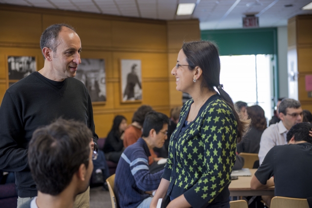
Assignments for Professor Saman Amarasinghe’s undergraduate course included consulting with mentors, interviewing users, writing promotional plans, — and, of course, leading the development of an open-source apps. Image: MIT News

Larry Hardesty | MIT News


Date Posted: 

Monday, August 14, 2017 - 1:15pm

Card Title Color: 

Black

Card Description: 

New project-based course lets undergrads lead the development of open-source software.

Photo: 

Card Wide Image: 

Viewing all 1281 articles
Browse latest View live


<script src="https://jsc.adskeeper.com/r/s/rssing.com.1596347.js" async> </script>